semi合集-English.pdf - 第176页
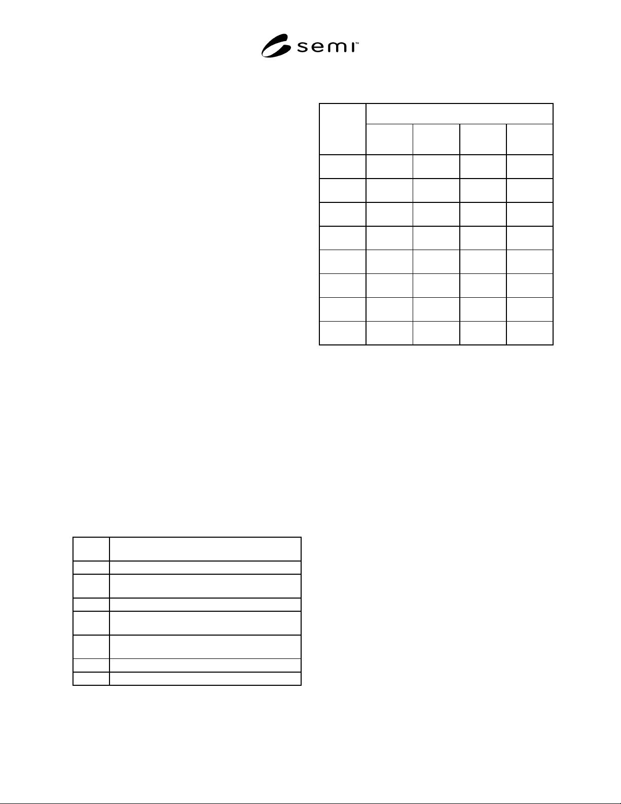
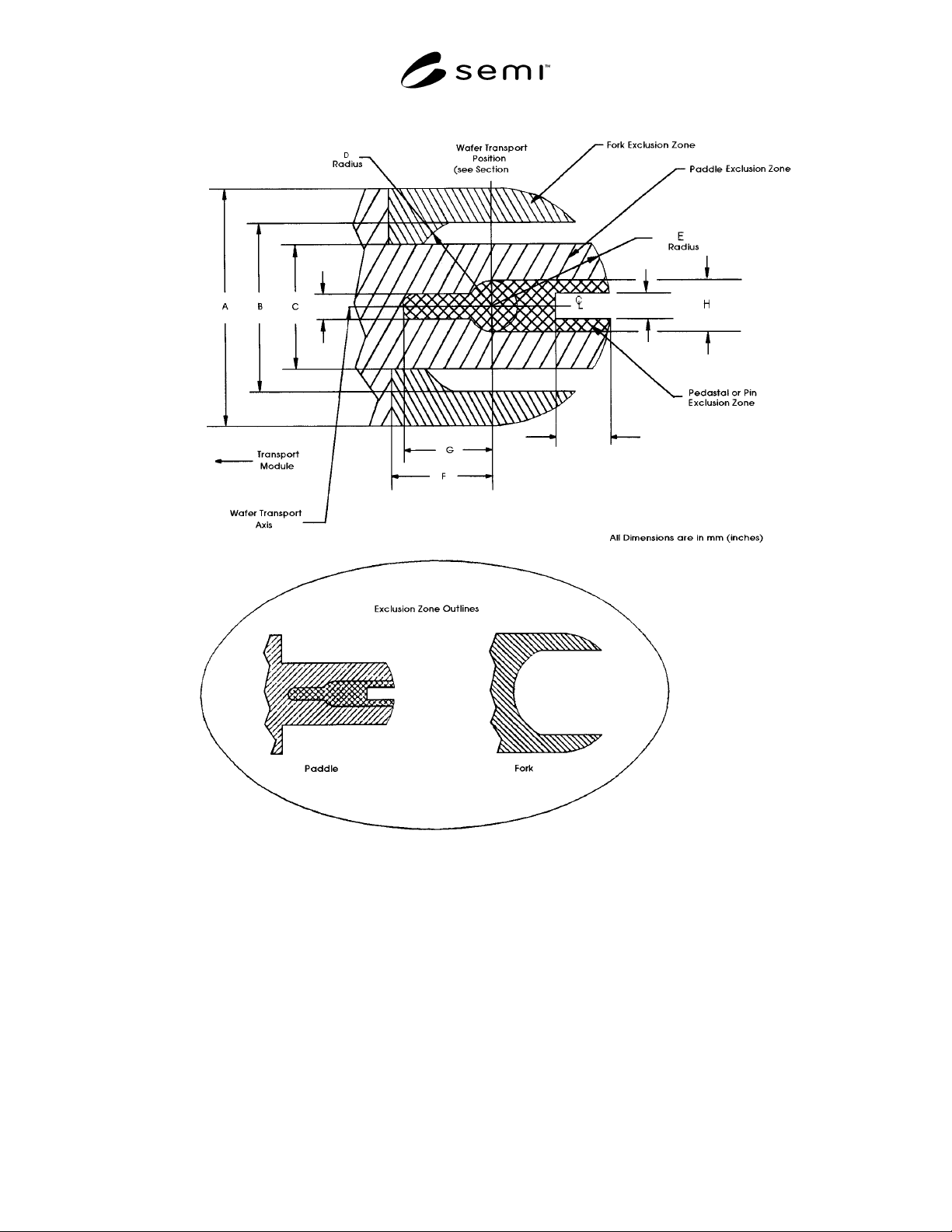
SEMI E22-0697 © SEMI 1991, 2002 3 5.1 .9) 10 (0.39 ) 10 (0.39 ) 25 (0.98 ) Figure 1 Wafer Transport Plane Exclusion Zone (P lan View)
SEMI E22-0697 © SEMI 1991, 2002 2
of the paddle exclusion zone to accommodate a pedestal
and or pin(s) in a process or cassette module (referred
to as a pedestal or pin exclusion zone).
6.3 Maximum Pedestal Diameter — The diameter is
not to exceed dimension H given in Table 2.
6.4 Pin Location — Wafer support pins to be located
relative to the wafer transport plane exclusion zone.
The pins are to be located at radii dependent upon wafer
diameter as specified in Table 2.
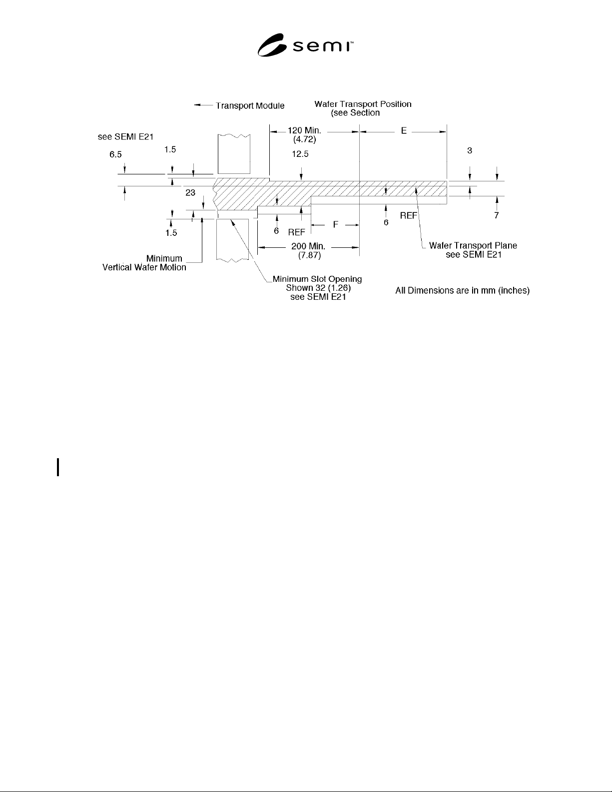
6.5 Vertical Plane Exclusion Zone — The extent of the
exclusion zone in the vertical plane is indicated by the
hatched area and the dashed outline in Figure 2. The
maximum extent of the exclusion zone allows the
transport module end effector to clear the minimum
wafer transport zone at the interface plane (see Related
Information R1-3). The vertical plane exclusion zone is
decreased in height in the vicinity of the wafer transport
position to allow the presence of shields, electrodes,
etc. in the process or cassette module.
6.6 Transport Module End Effector Exclusion Volume
— The exclusion volume within a process or cassette
module reserved for access by the transport module end
effector is defined by the intersection of the two
orthogonal exclusion zones described in Sections 6.2
and 6.5. This exclusion volume allows the transport
module end effector to accept or present a wafer at the
wafer transport position within a process or cassette
module (see Related Information R1-4).
LIST OF FIGURES
Figure 1. Wafer Transport Plane Exclusion Zone (Plan
View)
Figure 2. Vertical Plane Exclusion Zone (Elevation
View)
Table 1 Wafer Transport Plane Exclusion Zone
Variables
A Maximum width of the wafer transport plane
exclusion zone
B Minimum outside clearance for support pins
C Maximum inside clearance for support pins
and/or slot
D Minimum radial clearance for support pins
E Outermost radius of wafer transport plane
exclusion zone
F Minimum clearance for entry into SEMI
Standard Wafer Carrier
G Maximum clearance for support pins
H Maximum clearance for support pedestal
Table 2 Wafer Transport Plane Exclusion Zone
Dimensions
Wafer Size
Variables
100 mm
(4 in.)
125 mm
(5 in.)
150 mm
(6 in.)
200 mm
(8 in.)
A 120 mm
(4.72 in.)
145 mm
(5.71 in.)
170 mm
(6.69 in.)
220 mm
(8.66 in.)
B 86 mm
(3.39 in.)
107 mm
(4.21 in.)
129 mm
(5.08 in.)
172 mm
(6.77 in.)
C 50 mm
(1.97 in.)
66 mm
(2.60 in.)
78 mm
(3.07 in.)
104 mm
(4.09 in.)
D 47 mm
(1.85 in.)
60 mm
(2.36 in.)
72 mm
(2.83 in.)
97 mm
(3.82 in.)
E 60 mm
(2.36 in.)
72 mm
(2.83 in.)
85 mm
(3.35 in.)
110 mm
(4.33 in.)
F 70 mm
(2.76 in.)
82 mm
(3.23 in.)
95 mm
(3.74 in.)
120 mm
(4.72 in.)
G 47 mm
(1.85 in.)
60 mm
(2.36 in.)
72 mm
(2.83 in.)
97 mm
(3.82 in.)
H 30 mm
(1.18 in.)
38 mm
(1.50 in.)
45 mm
(1.77 in.)
60 mm
(2.36 in.)
SEMI E22-0697 © SEMI 1991, 2002 3
5.1.9)
10
(0.39)
10
(0.39)
25
(0.98)
Figure 1
Wafer Transport Plane Exclusion Zone (Plan View)
SEMI E22-0697 © SEMI 1991, 2002 4
(0.26)
(
0.06
)
(
0.49
)
5.9.1)
(0.12)
(
0.28
)
(0.236)
(
0.238
)
(0.91)
(
0.06
)
6.0
(
0.236
)
Capability see SEMI E21
Figure 2
Vertical Plane Exclusion Zone (Elevation View)
NOTICE: The user’s attention is called to the possibility that compliance with this standard may require use of an
invention covered by patent rights. By publication of this standard, Semiconductor Equipment and Materials
International (SEMI) takes no position respecting the validity of any patent rights asserted in connection with any
item mentioned in this standard. In particular, users of the specification should be aware that Drytek, Inc., A Unit of
General Signal, 16 Jonspin Road, Wilmington, MA 01887-1087, Phone: (508) 657-3933, has neither claimed nor
disclaimed that compliance with this specification would require use of an invention covered by one or more of its
patents. Users of this standard are expressly advised that determination of any such patent rights, and the risk of the
infringement of such rights, are entirely their own responsibility.
NOTICE: SEMI makes no warranties or representations as to the suitability of the standards set forth herein for any
particular application. The determination of the suitability of the standard is solely the responsibility of the user.
Users are cautioned to refer to manufacturer' s instructions, product labels, product data sheets, and other relevant
literature, respecting any materials or equipment mentioned herein. These standards are subject to change without
notice.
By publication of this standard, Semiconductor Equipment and Materials International (SEMI) takes no position
respecting the validity of any patent rights or copyrights asserted in connection with any items mentioned in this
standard. Users of this standard are expressly advised that determination of any such patent rights or copyrights, and
the risk of infringement of such rights are entirely their own responsibility.
.