semi合集-English.pdf - 第7455页
SEMI MF1535-1104 © SEMI 2004 13 RELATED INFORMATION 2 TEMPERATURE DEPENDENCE OF CARRIER RECOMBINATION LIFETIME NOTICE : This relat ed information is not an offici al part of SEMI MF1535. It was de rived from information …
SEMI MF1535-1104 © SEMI 2004 12
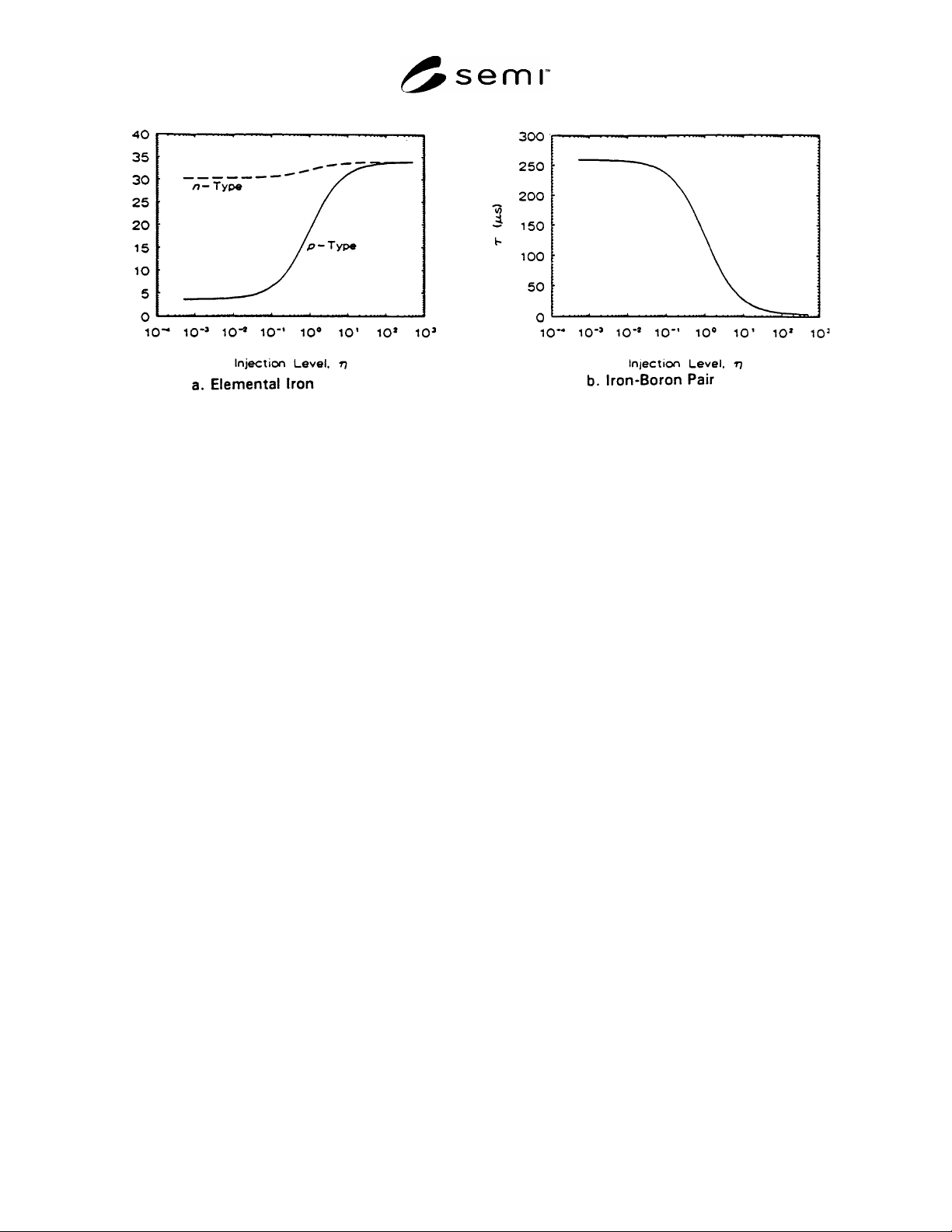
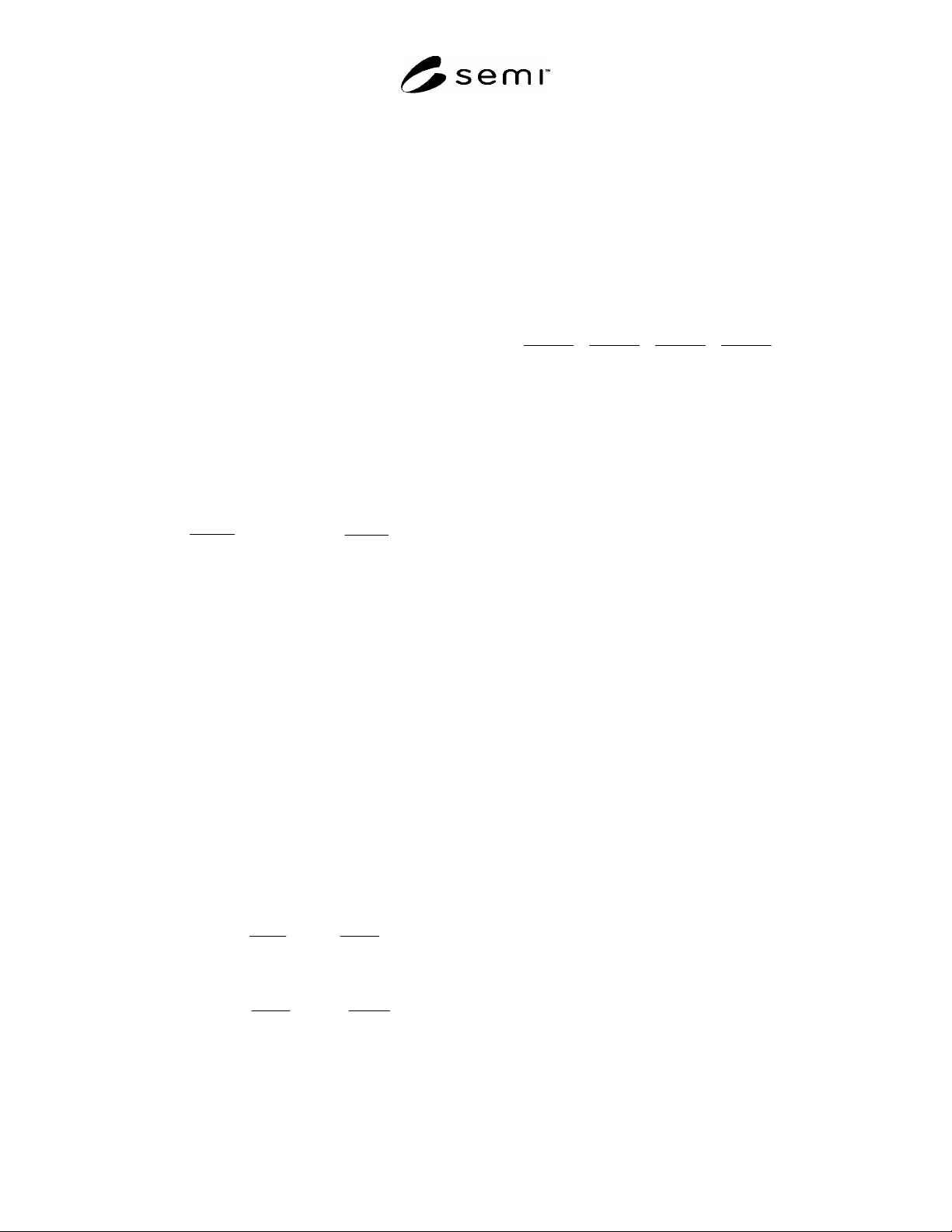
Figure R1-2
Recombination Lifetime as a Function of Injection Level
SEMI MF1535-1104 © SEMI 2004 13
RELATED INFORMATION 2
TEMPERATURE DEPENDENCE OF CARRIER RECOMBINATION
LIFETIME
NOTICE: This related information is not an official part of SEMI MF1535. It was derived from
information developed during the original preparation of the standard in ASTM Committee F-1 in 1994.
This related information was approved for publication by full letter ballot procedures.
R2-1 The temperature dependence of the carrier
recombination lifetime as determined under low-
injection conditions has been proposed
4
as a means for
identifying metallic impurities in silicon. However, this
is possible only for low injection and then only under
very restricted conditions.
R2-2 In the low-injection limit, the (S-R-H) carrier
recombination lifetime is given by Equation R1-2. In a
nondegenerate semiconductor, the carrier densities, n
0
,
p
0
, n
1
, and p
1
, are all exponential functions of
temperature. The equilibrium electron and hole
densities, n
0
and p
0
, respectively, are given as follows:
kT
Nn
cF
c
exp
0
and
kT
Np
Fv
v
exp
0
(R2-1)
where:
N
c
= the density of states in the conduction band, in
states/cm
3
,
N
v
= density of states in the valence band, in
states/cm
3
,
F
= Fermi energy, or the equilibrium electrochemical
potential, in eV,
c
= conduction band edge, in eV,
v
= valence band edge, in eV,
k =
Boltzmann's constant ( = 8.6173 × 10
5
eV/K),
and
T = temperature, in K.
Similarly, the electron (n
1
) and hole ( p
1
) densities when
the Fermi energy is at the defect center energy
T
are
given as follows:
kT
n
kT
Nn
FT
cT
c
expexp
01
and
kT
p
kT
Np
TF
Tv
v
expexp
01
(R2-2)
R2-3 From Equation R1-2, it is clear that the low-
injection (or small-signal) carrier recombination
lifetime,
0
, can be calculated readily in terms of the
electron and hole capture time constants,
n0
and
p0
, as
the sum of four terms:
00
10
00
00
00
10
00
00
0
np
n
np
n
np
p
np
p
pp
nn
(R2-3)
In the temperature region between the freeze-out region
and the intrinsic region where the majority carrier
density is equal to the net dopant density, the
denominator of these terms is constant. If, in addition,
the capture time constants are assumed not to depend
on temperature, the slope of the ln
0
versus 1/T curve
yields the defect center energy,
T
, in those temperature
regions where the defect centers are partially filled (that
is, when a term in p
1
or n
1
dominates the small-signal
recombination lifetime). Although this assumption is
usually not rigorously correct, the variation of capture
time constant with temperature is usually much less
strong than the exponential dependence of the carrier
densities.
R2-4 Three examples, elemental iron in both n- and p-
type silicon and iron-boron pairs in p-type silicon, serve
to illustrate these considerations. In each case the iron
density is assumed to be 5 × 10
11
atoms/cm
3
and the
dopant density is assumed to be 1 × 10
15
atoms/cm
3
, for
p-type silicon this dopant density corresponds to a
resistivity
10–15 ·cm and for n-type silicon it
corresponds to a resistivity 3–5 ·cm. The
temperature range considered is from 250 to 1000 K
over which the dopant atoms may be assumed to be
fully ionized. Elemental iron is a donor center which,
as shown in Table R1-1, lies well above the valence
band edge in the bottom half of the forbidden energy
gap. The iron-boron pair is also a donor center but it
lies much closer to the top of the valence band.
Consequently, in each case p
1
>> n
1
, the difference
being greater for the iron-boron pair.
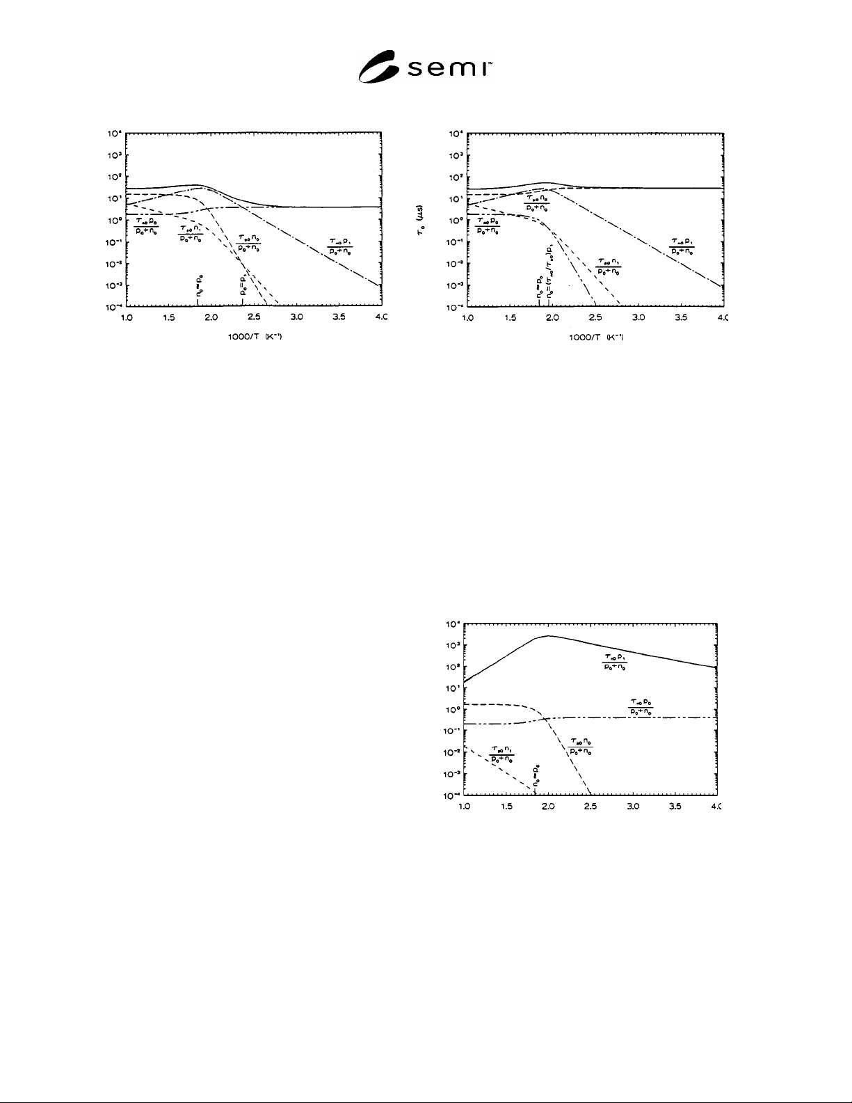
R2-4.1 Elemental Iron in p-Type Silicon (see Figure
R2-1) — Below room temperature, p
0
>> p
1
>> n
1
>>
n
0
, so
0
=
n0
. Between about 150°C and about 200°C,
p
1
> p
0
> n
0
and the term p
1
is the largest single term.
However, because there is not much difference between
p
1
and p
0
, the slope of the
0
curve never quite reaches
that of the p
1
term, and thus the energy of the elemental
iron center cannot be determined accurately from the
curve. At still higher temperatures, n
0
becomes
SEMI MF1535-1104 © SEMI 2004 14
comparable with p
0
(approaching the intrinsic
condition) and the carrier recombination lifetime
decreases; however, no single term dominates the
expression and so the slopes have no physical meaning.
R2-4.2 Elemental Iron in n-Type Silicon (see Figure
R2-2) — Below about 100°C, n
0
>> p
1
>> n
1
>> p
0
, so
0
=
p0
. Between about 200°C and about 225°C, p
1
>
n
0
> p
0
and the term p
1
is again the largest single term.
In this case, there is even less difference between the
terms in
p
1
and p
0
, so the slope of the
0
curve is never
dominated by a single term, and thus the energy of the
elemental iron center cannot be determined from the
curve. At still higher temperatures, p
0
becomes
comparable with n
0
(approaching the intrinsic
condition) and the carrier recombination lifetime
decreases; however, as for near-intrinsic p-type
material, no single term dominates the expression and
so the slopes have no physical meaning.
R2-4.3 Iron-Boron Pairs in p-Type (Boron-Doped)
Silicon (see Figure R2-3) — In this case, p
1
>> p
0
>>
n
0
>> n
1
, so that the term in p
1
dominates the low-
injection recombination lifetime at all temperatures
from well below room temperature to about 225°C.
Since
p
0
= N
boron
,
0
n0
(p
1
/N
boron
), so that the negative
slope of a plot of ln
0
against 1/T yields
=
FeB
v
,
the activation energy of the iron-boron pair. At higher
temperatures, the material becomes near-intrinsic and
the denominator increases, resulting in a decrease in
0
.
R2-5 These examples illustrate the limited range of
conditions over which the activation energy obtained
from measurements of carrier recombination lifetime as
a function of temperature slightly above room
temperature can be associated with the energy level of a
defect center located near the middle of the forbidden
energy gap, as are most of the elemental metallic
impurities.
Figure R2-3
Low-Injection Recombination Lifetime (solid curve)
as a Function of Reciprocal Temperature for Iron-
Boron in p-Type Silicon
Figure R2-1
Low-Injection Recombination Lifetime
(solid curve) as a Function of Reciprocal
Temperature for Elemental Iron in
p-Type Silicon
Figure R2-2
Low-Injection Recombination Lifetime
(solid curve) as a Function of Reciprocal
Temperature for Elemental Iron in
n-Type Silicon