semi合集-English.pdf - 第7513页
SEMI MF1724-1104 © SEMI 2004 8 NOTICE: SEMI makes no warranties or represen tations as to the suitability o f the standards set forth herein for any particular application . The determinati on of the suitability o f the …
SEMI MF1724-1104 © SEMI 2004 7
14.2.2 Method variation was determined by analyzing
the 10-ppb digested control standards over a period of
one year. Instrument readings of concentration values
are about 10 g/L. The standard deviation of this set of
values represents the variation due to metals retention
efficiency, reagent purity, apparatus purity, environ-
ment purity, and analyst technique.
14.2.3 Lot sample analysis variation was determined
by analyzing polysilicon lot samples over a one-year
period. The standard deviation of this set of analyses
represents the variation due to sampling techniques,
contamination during sampling and processing of lots,
and the total analytical method variation.
14.2.4 The standard deviations in these studies are
summarized in Table 2.
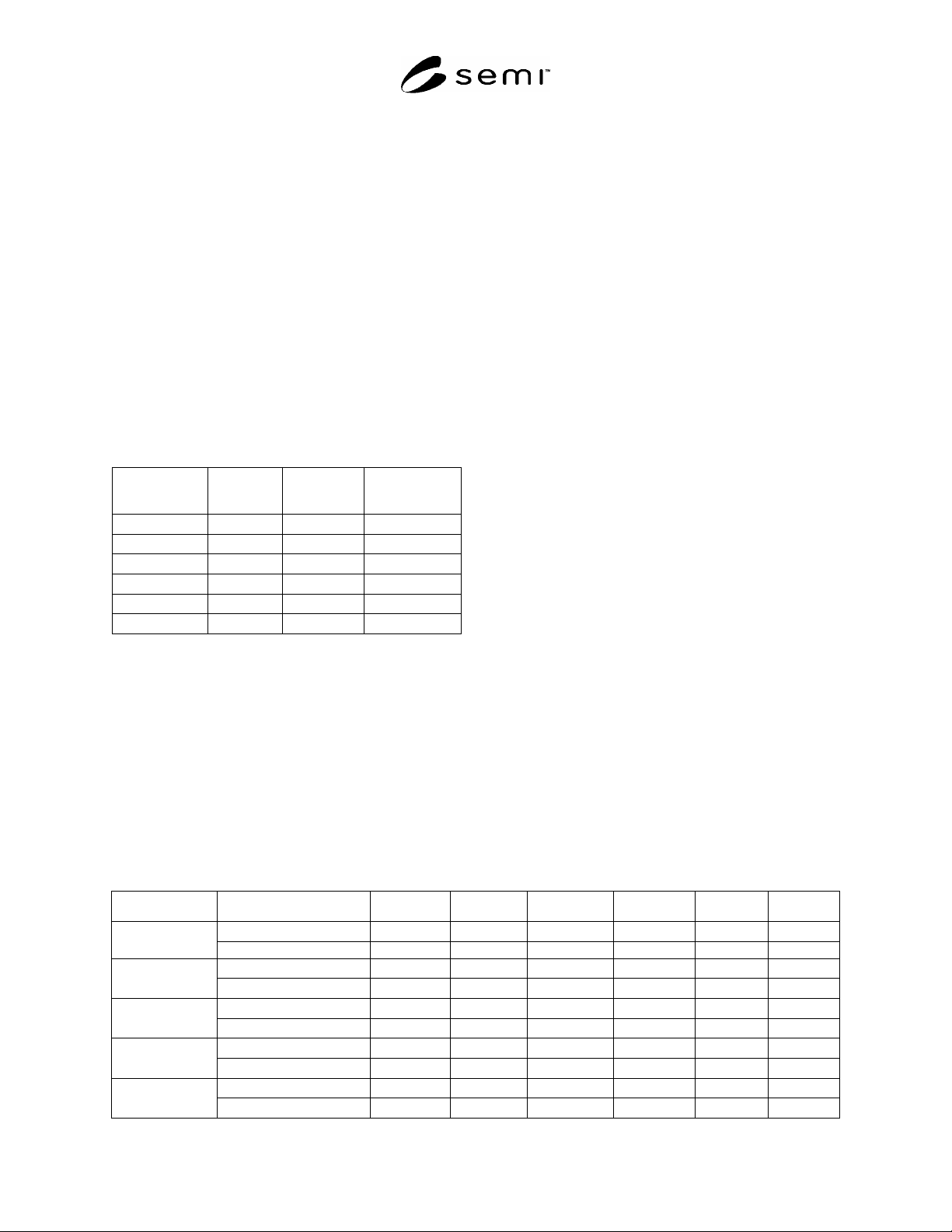
Table 2 Standard Deviation (ppbw) Values for a
One-Laboratory Study of Variations for a One-Year
Period
Analyte
Instrument
Variation
Method
Variation
Lot Sample
Variation
Sodium 0.01 0.08 0.15
Aluminum <0.01 0.10 0.28
Iron <0.01 0.10 0.13
Chromium <0.01 0.05 <0.01
Nickel <0.01 0.03 <0.01
Zinc <0.01 0.08 0.13
14.3 Interlaboratory Variation — Interlaboratory
correlation studies were conducted to test the ability of
the method to analyze surface contamination in
polysilicon lots at the sub-ppbw level. Each laboratory
used different polysilicon sample weights, acid
mixtures, and dilution factors, but all performed the
analyses in clean rooms with high purity reagents, and
calibration controls. All polysilicon samples were
supplied by Laboratory A, with lots chosen to be
representative of polysilicon with only trace
contaminants, at sub-ppbw levels. No samples with
added contaminants were supplied; this correlation
study was to determine variation at these levels due to
sampling, the different analytical procedures, and
different laboratory environments. Laboratory A
followed this test method, while Laboratories B, C, D,
and E used variations of this test method and the acid
mixture and dilution factor for these laboratories were
not reported. The ability of the method to detect values
above the sub-ppbw level is determined by the recovery
of the control standards as discussed in Section 14.2.
Requested weights of samples were taken from a
polysilicon lot, sealed in double polyethylene bags, and
sent to the labs for analysis.
14.3.1 Laboratory A and Laboratory B used 300-g
sample weights. Five polysilicon lots were analyzed.
Detection limits for Laboratory A are based on 3 sigma
of the method variation listed in Table 2.
14.3.2 Laboratory C used 200-g sample weights. Five
polysilicon lots were analyzed.
14.3.3 Laboratory D used 200-g sample weights.
Seven polysilicon lots were analyzed.
14.3.4 Laboratory E used 80-g sample weights. Three
polysilicon lots were analyzed.
14.3.5 In each case, the average value and standard
deviation are given for each analyte reported. Values
less than the detection limit are reported as <“detection
limit” and no standard deviation is reported. Results
are tabulated in Table 3.
14.4 Bias — Although liquid standard samples are
available, no reference materials of contaminated
silicon are available to calibrate this measurement;
therefore, no bias statement is possible.
15 Keywords
15.1 acid extraction; contamination; graphite furnace
atomic absorption spectroscopy; metals; polycrystalline
silicon; surface contamination
Table 3 Surface Metals Analysis Comparison (ppbw) for a Five-Laboratory Correlation Study
Laboratory Sodium Aluminum Iron Chromium Nickel Zinc
Average <0.24 <0.30 <0.30 <0.15 <0.09 <0.24 Laboratory A
Standard Deviation … … … … … …
Average 0.23 0.27 0.03 <0.01 <0.06 0.09 Laboratory B
Standard Deviation
0.03 0.04 0.02 … … 0.03
Average 0.04 0.02 0.11 0.02 0.02 0.04 Laboratory C
Standard Deviation
0.01 <0.01 0.07 <0.01 0.01 0.01
Average 0.18 … 0.12 0.02 0.02 0.20 Laboratory D
Standard Deviation
0.07 … 0.07 0.02 0.02 0.05
Average <0.20 <0.25 <0.10 <0.13 <0.20 0.12 Laboratory E
Standard Deviation … … … … …
0.06

SEMI MF1724-1104 © SEMI 2004 8
NOTICE: SEMI makes no warranties or representations as to the suitability of the standards set forth herein for any
particular application. The determination of the suitability of the standard is solely the responsibility of the user.
Users are cautioned to refer to manufacturer's instructions, product labels, product data sheets, and other relevant
literature, respecting any materials or equipment mentioned herein. These standards are subject to change without
notice.
By publication of this standard, Semiconductor Equipment and Materials International (SEMI) takes no position
respecting the validity of any patent rights or copyrights asserted in connection with any items mentioned in this
standard. Users of this standard are expressly advised that determination of any such patent rights or copyrights, and
the risk of infringement of such rights are entirely their own responsibility.
Copyright by SEMI® (Semiconductor Equipment and Materials
International), 3081 Zanker Road, San Jose, CA 95134. Reproduction of
the contents in whole or in part is forbidden without express written
consent of SEMI.

SEMI MF1725-1103 © SEMI 2003 1
SEMI MF1725-1103
PRACTICE FOR ANALYSIS OF CRYSTALLOGRAPHIC PERFECTION
OF SILICON INGOTS
This standard was technically approved by the Global Silicon Wafer Committee and is the direct
responsibility of the North American Silicon Wafer Committee. Current edition approved for publication by
the North American Regional Standards Committee on September 16, 2003. Initially available at
www.semi.org October 2003; to be published November 2003. Originally published by ASTM International
as ASTM F 1725-97. Last previous edition ASTM F 1725-02.
1 Purpose
1.1 The use of silicon wafers in many semiconductor
devices requires a consistent atomic lattice structure.
Crystal defects disturb local lattice energy conditions
that are the basis for semiconductor behavior. These
defects have distinct effects on essential semiconductor
device-manufacturing processes such as alloying and
diffusion.
1.2 This practice provides guidance regarding
procedures for analysis of crystal defects of silicon
ingots from which silicon wafers are cut.
1.3 This practice together with the referenced standards
may be used for process control, research and
development, and materials acceptance purposes.
2 Scope
2.1 This practice covers the analysis of the
crystallographic perfection in silicon ingots. The steps
described are sample preparation, etching solution
selection and use, defect identification, and defect
counting.
2.2 This practice is suitable for use in evaluating
silicon grown in either the [111] or the [100] direction
and doped either p or n type with resistivity greater than
0.005 Ω·cm.
NOTICE: This standard does not purport to address
safety issues, if any, associated with its use. It is the
responsibility of the user of this standard to establish
appropriate safety and health practices and determine
the applicability of regulatory or other limitations prior
to use.
3 Referenced Standards
3.1 SEMI Standards
SEMI C18 — Specification for Acetic Acid
SEMI C28 — Specifications and Guidelines for
Hydrofluoric Acid
SEMI C35 — Specifications and Guidelines for Nitric
Acid
SEMI MF26 — Test Method for Determining the
Orientation of a Semiconductor Single Crystal
SEM MF523 — Practice for Unaided Visual Inspection
of Polished Silicon Wafers
SEMI MF1241 — Terminology of Silicon Technology
SEMI MF1809 — Guide for Selection and Use of
Etching Solutions to Delineate Structural Defects in
Silicon
SEMI MF1810 — Test Method for Counting
Preferentially Etched or Decorated Surface Defects in
Silicon Wafers
3.2 ASTM Standard
D 5127 — Guide for Ultra Pure Water Used in the
Electronics and Semiconductor Industry
1
NOTICE: Unless otherwise indicated, all documents
cited shall be the latest published versions.
4 Terminology
4.1 Defect-related terminology may be found in SEMI
MF1241.
5 Summary of Practice
5.1 The end portion of the silicon crystal, which
solidified last, may contain dislocations or other defects
such as slip. The portion containing the defects is
removed by sawing the crystal. A specimen wafer from
the end of the remaining ingot is obtained with a second
cut.
5.2 This wafer is mechanically lapped, chemically
polished, and then etched in a preferential defect
etching solution.
5.3 The etched surface is examined under bright light
illumination and examined microscopically to count
and classify the imperfections highlighted by the
preferential defect etching solution.
1 Annual Book of ASTM Standards, Vol 11.01. ASTM International,
100 Barr Harbor Drive, West Conshohocken, PA 10428, USA.
Telephone: 610-832-9585, Fax: 610-832-9555. Website:
www.astm.org