semi合集-English.pdf - 第7221页
SEMI MF43-0705 © SEMI 2003, 2005 4 NOTE 4: Detailed procedures for in situ determination of the spacing betw een adjacent probes of an in-line four-point probe are given in the Probe Assembly paragraph of the Suitability…
SEMI MF43-0705 © SEMI 2003, 2005 3
4.4 DIN Standards
50430 — Measurement of the Specific Electrical Resistivity of Silicon or Germanium Single Crystals in Bars Using
the Two-probe Direct Current Method
4
50431 — Measurement of the Electrical Resistivity of Silicon or Germanium Single Crystals by Means of the Four-
point-probe Direct Current Method with Collinear Four-probe Array
4
NOTICE: Unless otherwise indicated, all documents cited shall be the latest published versions.
5 Terminology
5.1 Definitions
5.1.1 Terms relating to silicon and other semiconductor technology are defined in SEMI M59.
6 Summary of Test Methods
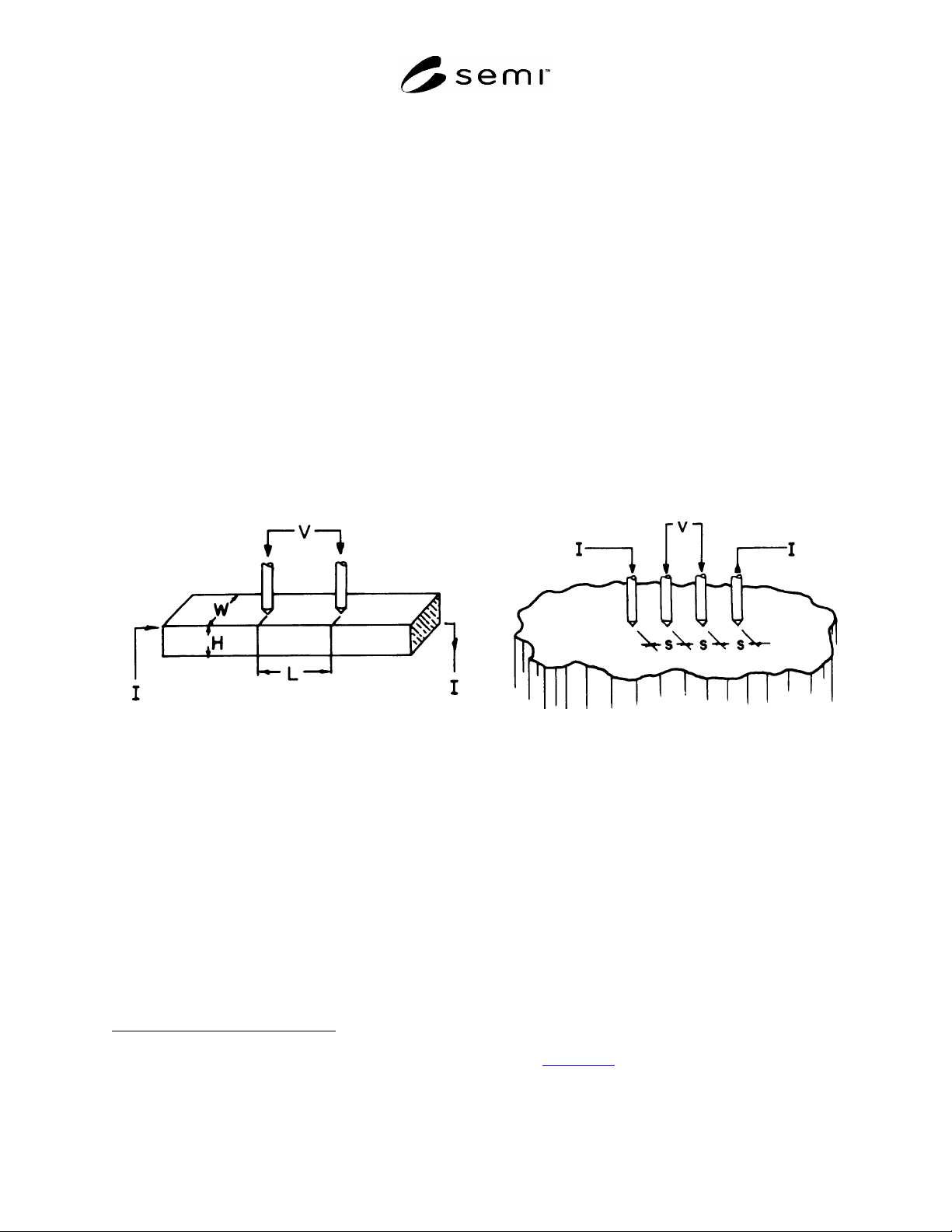
6.1 Two-Probe Method — A direct current, I, is passed through ohmic contacts at the ends of a bar specimen and
the potential difference, V, is determined between two probes placed along the current direction (Figure 1). The
resistivity,
, is calculated from the current and potential values and factors appropriate to the geometry.
6.2 Four-Probe Method — An in-line four-point probe is placed on a flat surface of a solid specimen which can be
approximated as semi-infinite. A direct current, I, is passed through the specimen between the outer probes and the
resulting potential difference, V, is measured between the inner probes (Figure 2). The resistivity,
, is calculated
from the current and potential values and factors appropriate to the geometry.
4 Deutches Institut für Normung e.V., standards are available in both English and German editions from Beuth Verlag GmbH, Burggrafenstrasse
6, 10787 Berlin, Germany, Telephone: 49.30.2601-0, Fax: 49.30.2601.1263, Website:
www.beuth.de.
Figure 1
Specimen and Probe Arrangement for Two-Probe
Measurements on a Rectangular Bar
Figure 2
Specimen and Probe Arrangement for Four-Probe
Measurements on a Semi-Infinite Solid Specimen
7 Apparatus
7.1 Jigs — Suitable for mounting the specimens and contacting them with either two or four probes as required.
7.1.1 Probes — Shall be individually spring mounted and shall be loaded with a force of 1.5 ± 0.5 N. The probes
may be made from hardened tool steel, tungsten carbide, or other conducting metal and may be chisel shaped for
measurement of curved surfaces or pointed for measurement on flat sections. In the case of point probes, the
nominal radius of the tips shall be initially 25 to 50 m. With all probing devices, frequent checking of the probe
spacing with a calibrating microscope is desirable. Probes shall be replaced or resharpened when necessary to
maintain the required spacing tolerance. Isolation resistance between the probes shall be at least 10
9
.
SEMI MF43-0705 © SEMI 2003, 2005 4
NOTE 4: Detailed procedures for in situ determination of the spacing between adjacent probes of an in-line four-point probe are
given in the Probe Assembly paragraph of the Suitability of Test Equipment section of SEMI MF84. These procedures, for
which equipment described in the Probe Alignment and Separation paragraph of the Apparatus section of SEMI MF84 is
required, can be used to establish probe spacings and their repeatability for both two- and four-probe assemblies. When four-
probe measurements are made on semi-infinite solids, the probe spacing correction factor, F
sp
, in Equation 5 of the Suitability of
Test Equipment section, of SEMI MF84 should be replaced by:
s
s
F
sp
2
12511 . (1)
where:
s
2
= spacing between inner pair of probes, cm, and
s = average probe spacing, cm.
In general, however, the correction for unequal probe spacing is neglected.
7.1.2 Probe Mountings — Shall be furnished with appropriate guides to ensure that the probes contact the
specimen reproducibly with a probe spacing tolerance of ±0.5%.
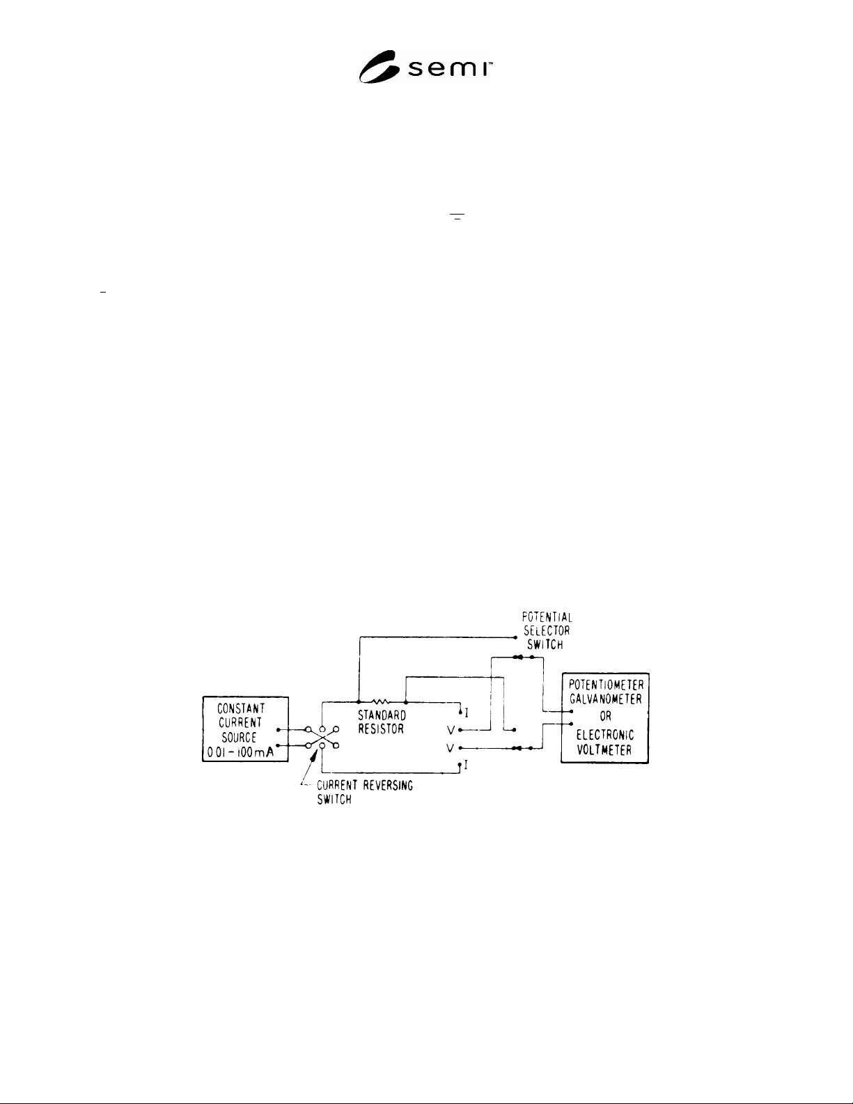
7.2 Electrical Circuit (see Figure 3)
7.2.1 Constant Current Source — Capable of supplying currents between 10
1
and 10
5
A. The current must be
known and maintained constant to ±0.5% during the measurement.
7.2.2 Current Reversing Switch
7.2.3 Standard Resistor — With a resistance within a factor of 100 of that of the specimen. (See Note 5.)
7.2.4 Double-Throw, Double-Pole Potential Selector Switch. (See Note 5.)
7.2.5 Potentiometer-Galvanometer or Electronic Voltmeter — Capable of measuring potential differences between
10
4
and 1 V of either polarity to ±0.5%. The input impedance must exceed 1000 times the total contact plus bulk
resistance of the specimen.
NOTE 5: The standard resistor and potential selector switch are not required for routine four-probe measurements if a calibrated
current source is used.
NOTE: The standard resistor and potential selector switch are not required for routine
four-probe measurements if a calibrated current source is used.
Figure 3
Recommended Electrical Circuit for Two-Probe and Four-Probe Resistivity Measurements
NOTE 6: The electrical measuring circuit may also measure either resistance or current directly. Any electrical circuit that
meets the requirements of the Electrical Equipment part of the Suitability of Test Equipment section, of SEMI MF84 is
acceptable for use in this test method. If the procedures of SEMI MF84 are used to evaluate the adequacy of the electrical
equipment, an appropriate analog test circuit as described in the Analog Test Circuit paragraph of the Apparatus section of
SEMI MF84 is required.

SEMI MF43-0705 © SEMI 2003, 2005 5
7.3 Lapping or Sandblasting Facilities — to provide a flat, abraded surface on which the measurement is made.
7.4 Micrometer or Vernier Caliper — to determine the cross-sectional area normal to the current in the two-probe
method to ±0.5% or for measuring the dimensions of circular specimens with thickness more than one, but less than
four, times the probe spacing in the four-probe method.
7.5 Thermometer — or other temperature measuring instrument to determine the ambient temperature to ±0.5°C.
8 Test Specimen
8.1 Two-Probe Method — The test specimen for the two-probe test method may be in the form of a strip, rod, or
bar. The ratio of the length to the larger cross-sectional dimension of the specimen shall be not less than 3 to 1. The
cross section of the specimen must be of measurable shape and should be as uniform as possible. Prior to
measurement, ohmic contact shall be made to the ends of the specimen (for example, by electroplating with copper
or nickel or by ultrasonic soldering). Connections to the ends may be made either with soldered leads or pressure
contacts.
NOTE 7: Alternative methods for forming ohmic contacts to germanium, silicon, and gallium arsenide are given in ASTM Test
Method F 76.
8.2 Four-Probe Method — One reasonably flat surface for the contacting probes is required on the specimen which
may be of any size or shape which approximates a semi-infinite solid. The conditions for a semi-infinite solid are
approximated within 2% when the thickness of the specimen and the distance from any probe to the nearest edge are
both at least four times the probe spacing.
8.2.1 If the specimen is of circular cross section and has thickness more than one, but less than four, times the
probe spacing, measure the thickness and diameter as follows:
8.2.1.1 Measure and record five values of thickness, w
i
, at various points near the center of the specimen according
to SEMI MF533 and calculate and record the average thickness, w:
5
1
5
1
i
i
ww (2)
8.2.1.2 Measure and record three values of the specimen diameter, D
i
, at the appropriate locations defined in
SEMI MF2074, and calculate and record the average diameter, D:
3
1
3
1
i
i
DD (3)
8.3 The surface on which the resistivity is determined with either the two- or four-probe test method shall be
abraded by lapping with No. 600 alumina or by sandblasting with No. 280 Carborundum, and the measurement shall
be made thereafter without unnecessary delay. The specimen shall show no surface cracks or other defects
observable with normal vision and it shall be free of surface oxide. The abrasive grain sizes specified for this
purpose shall comply with the appropriate ANSI Specification B74.10.
NOTE 8: The surface preparation procedure in the Preparation of Test Specimen section of SEMI MF84 is also acceptable.
9 Procedure
9.1 Measure and record the ambient temperature. Maintain the specimen at this temperature for a time sufficient
for it to come to equilibrium.
NOTE 9: The time required for equilibrium of a specimen depends on the mass of the specimen. For small specimens 30 min to
1 h should suffice. For large ingots 1 to 2 days may be required.
9.2 Two-Probe Method
9.2.1 Measure the cross-sectional area of the specimen in cm
2
and record as A.
9.2.2 Connect the current leads of the electrical measuring circuit to the ends of the specimen, place the potential
probes on the abraded surface, and adjust the current so that the electric field in the specimen does not exceed 1
V/cm.