semi合集-English.pdf - 第6275页
SEMI G54-93 © SEMI 1993 3 Table 1 Toleranc e Limits Dimension (Tolera nce) PDIP PLCC SOIC PQFP PTAB UNITS Packa ge Leng th/Width ± 0.002 ( 0.05) 0.002 (0.05) 0.002 (0.05) 0.002 (0.05) 0.002 (0.05) in. (mm) Cav ity Mism a…

SEMI G54-93 © SEMI 1993 2
3.9 Overlap — the difference in length or width
between the top and bottom cavities. Overlap may be a
feature designed into the mold to avoid mismatch (see
Figure 5). All statements regarding overlap of cavities
are applicable to both the X and Y axis. All
measurements are made prior to lead trim and form.
3.10 Package Warpage — loss of planarity of a
molded surface excluding protrusions and intrusions
(see Figure 7). Each package type has a maximum
allowable warpage and a warp factor is used to
determine the maximum warpage for a particular
package dimension. The Warp Factor (WF) is defined
as follows:
WF =
Total Warp in inches (mm
)
×1000
Package dimension in inches (mm)
Package warpage is usually caused by incorrect
package design and/or poor molding conditions.
3.11 Parting Line Protrusions, or Intrusions — plastic
excesses (flash) or losses (chips or voids) at the parting
line after normal processing to mold, deflash, trim, and
singulate the packages.
3.12
Surface Protrusions or Intrusions — plastic
excesses (bumps or blisters) or recesses (pits or voids)
on any surface of the package.
4 Ordering Information
Purchase orders for molded plastic tooling furnished to
this document, shall include the following items:
4.1 A package tooling outline drawing showing all the
required dimensions listed in Section 5. The molded
surface finish(es) and the lead finish shall be specified.
4.2
The plastic compound to be used shall be
specified. If the compound is proprietary, then the
molding and molded characteristics shall be supplied.
4.3 The leadframe drawing detailing the material, all
dimensions, and, if applicable, lead finish pre-plate
specifications.
4.4
The type and part number of the molding and trim,
form, singulate press to be used.
4.5 Singulation or off-load requirements.
4.6 Expectations of Tooling Performance — Tooling
performance is not limited to the items listed in Section
5 and 6. Any other customer requirements, such as the
limits on wire sweep, resin bleed or internal voiding,
shall also be included with the purchase order.
4.7
Reference to this specification.
4.8 Vendor certification requirements.
5 Dimensions
5.1 All package dimensions should be specified in
detail.
5.2 Ejector pin mark location from the package
centerline. This should include ejector pin sizes, depths,
and draft angles.
5.3
Pin 1 ID shape and location from the package
center with respect to the lead frame Pin 1 location.
5.4
All critical radii (unspecified radii, often shown
sharp on the drawing, may have the maximum radius
shown in the table of Section 6).
5.5
Plastic stand-off shape and locations from the
package center.
5.6
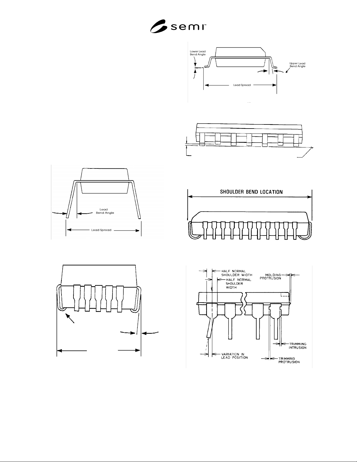
Lead spread (the distance between the outer edge
of opposing leads).
5.7 Shoulder bend location and lead bend angle
(optional).
5.8
Foot angle radius (maximum a nd minimum).
5.9 Foot length.
5.10 Lead length.
5.11 Shoulder width (maximum width should include
protrusion).
6 Dimensional Tolerance Li mits
These criteria, where applicable, apply only to opaque,
plastic molded semiconductor packages. If an item is
not mentioned in the following table, then the
tolerances on the dimensions of that item follow the
general tolerance limits stated on the drawing.
Dimensions are in inches (millimeters) except as noted.
Dimensions are to be verified per SEMI G48.
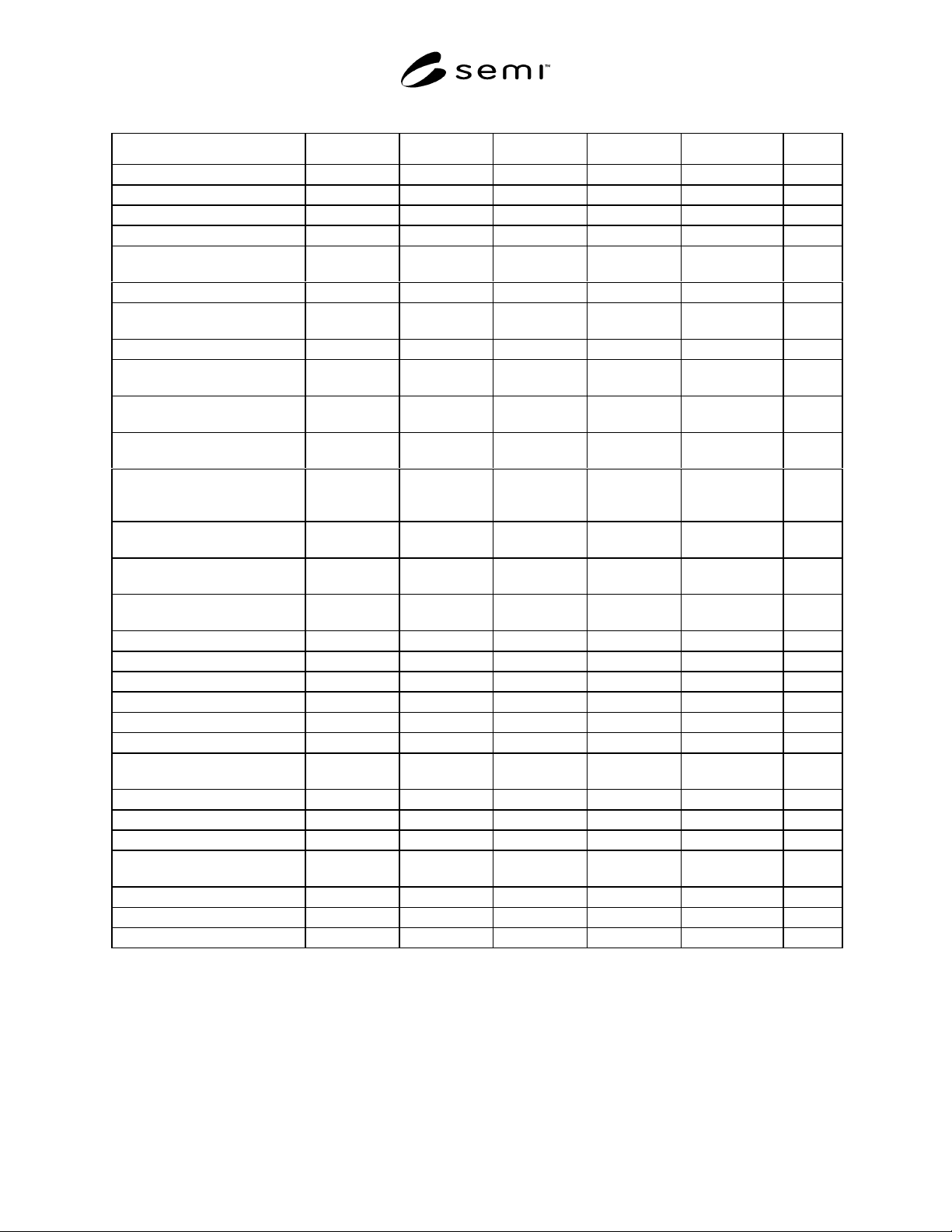
SEMI G54-93 © SEMI 19933
Table 1 Tolerance Limits
Dimension (Tolerance) PDIP PLCC SOIC PQFP PTAB UNITS
Package Length/Width ± 0.002 (0.05) 0.002 (0.05) 0.002 (0.05) 0.002 (0.05) 0.002 (0.05) in. (mm)
Cavity Mismatch ± 0.002 (0.05) 0.002 (0.05) 0.002 (0.05) 0.002 (0.05) 0.002 (0.05) in. (mm)
Cavity Overlap (Max.) 0.002 (0.05) 0.002 (0.05) 0.002 (0.05) 0.002 (0.05) 0.002 (0.05) in. (mm)
Package/Leadframe Offset ± 0.002 (0.05) 0.002 (0.05) 0.002 (0.05) 0.002 (0.05) 0.001 (0.025) in. (mm)
Plastic Body Thickness —
Top and Bottom ±
0.002 (0.05) 0.002 (0.05) 0.002 (0.05) 0.002 (0.05) 0.001 (0.025) in. (mm)
Surface Protrusions (Max.) 0.001 (0.025) 0.001 (0.025) 0.001 (0.025) 0.001 (0.025) 0.001 (0.025) in. (mm)
Surface Intrusions —
Depth (Max.)
0.001 (0.025) 0.001 (0.025) 0.001 (0.025) 0.001 (0.025) 0.001 (0.025) in. (mm)
-X-Y Dimension (Max.) 0.010 (0.25) 0.010 (0.25) 0.010 (0.25) 0.010 (0.25) 0.005 (0.127) in. (mm)
Ejector Pins — Intrusion only
(Max.)
0.010 (0.25) 0.010 (0.25) 0.010 (0.25) 0.008 (0.20) 0.005 (0.127) in. (mm)
Gate Feature — Intrusion only
(Max.)
0.020 (0.50) 0.020 (0.50) 0.010 (0.25) 0.020 (0.50) 0.002 (0.05) in. (mm)
Gate Feature — Protrusion only
(Max.)
0.004 (0.10) 0.004 (0.10) 0.004 (0.10) 0.004 (0.10) 0.004 (0.10) in. (mm)
Parting Line Protrusion — after
deflash dambar removal
(Max. per side)
0.006 (0.15) 0.006 (0.15) 0.006 (0.15) 0.006 (0.15) 0.005 (0.127) in. (mm)
Parting Line Intrusion —
Plastic (Max.)
0.010 (0.25) 0.010 (0.25) 0.005 (0.127) 0.010 (0.25) 0.005 (0.127) in. (mm)
Parting Line Protrusion —
after package singulation
0.006 (0.15) 0.006 (0.15) 0.006 (0.15) 0.006 (0.15) 0.005 (0.127) in. (mm)
Warp Factor (Max.) —
up to a Limit of
2.5% 0.003
(0.08)
2.5% 0.003
(0.08)
2.5% 0.003
(0.08)
2.5% 0.003
(0.08)
2.5% 0.003
(0.08)
in. (mm)
Draft Angles (Deg. ±) 1 1 1 1 1
Package Radii — Noted Radii ± 0.0025 (0.06) 0.0025 (0.06) 0.0025 (0.06) 0.0025 (0.06) * (*) in. (mm)
Shown Sharp (Max.) 0.020 (0.50) 0.020 (0.50) 0.010 (0.25) 0.020 (0.50) * (*) in. (mm)
Lead Spread ± 0.025 (0.64) 0.010 (0.25) 0.010 (0.25) 0.005 (0.127) * (*) in. (mm)
Lead Bend Angles (Deg. ±) - 5 2 2 2
Shoulder Bend Location ± 0.010 (0.25) 0.010 (0.25) 0.005 (0.127) 0.005 (0.127) * (*) in. (mm)
Lead Sweep (from True position
— Max.) (See Note 2)
0.007 (0.18) 0.004 (0.10) 0.004 (0.10) 0.003 (0.075) 0.003 (0.075) in. (mm)
Foot Length ± - - 0.005 (0.127) 0.005 (.127) * (*) in. (mm)
Foot Radius ± - 0.010 (0.25) - - - in. (mm)
Lead Length ± 0.005 (0.127) - - - - in. (mm)
Foot Width ±
incl. Leadframe Tolerance
- - 0.002 (0.05) 0.002 (0.05) * (*) in. (mm)
Lead Coplanarity (Max.) - 0.003 (0.08) 0.003 (0.08) 0.003 (0.08) 0.002** (0.05) in. (mm)
Dambar Trim Protrusions (Max.) 0.003 (0.08) 0.003 (0.08) 0.003 (0.08) 0.003 (0.08) 0.003 (0.08) in. (mm)
Dambar Trim Intrusions (Max.) 0.002 (0.05) 0.002 (0.05) 0.001 (0.025) 0.001 (0.025) 0.001 (0.025) in. (mm)
* To be determined.
** If applicable.
NOTE 2: SOIC, J leaded packages have the plastic bodies and leads evaluated to the SOIC and PLCC tolerances as appropriate.
NOTE 3: Lead Sweep is not acceptable at buy-off.
7 Sampling Plan
A sampling plan and buy-off procedure to determine compliance to the requirements of Sections 5 and 6 and other
relevant specifications shall be determined between vendor and customer.
SEMI G54-93 © SEMI 1993 4
8 Packaging and Marking
8.1 Packaging — Tooling must be packed in
containers designed and constructed to provide
protection against normal transportation damage risks
and spillage. The container will offer protection from
contamination and exposure to moisture. Tools may be
coated with a suitable rust inhibitor as agreed between
vendor and customer.
8.2
Marking — The following details shall be noted
on the packing slip:
Vendor Part Number
Customer Part Number
Shipping Date
Customer P.O. Number
Shipment Items
Figure 1A
PDIP Package
Foot
Radius
Lead
Bend Angle
Lead Spread
Figure 1B
PLCC Package
Figure 1C
SOIC and PQFP Packages
Vertical Lead
Position
Reference Plane
Figure 2
Lead Co-planarity
Figure 3
Shoulder Bend Location
Figure 4
Parting Line Protrusion, Lead Sweep and Lead
Shoulder Protrusions and Intrusions