semi合集-English.pdf - 第7879页
SEMI T13.1-1104 © SEMI 2004 3 Parameter Name SECS-II Data Item Reference SECS-II Format Remarks ServiceStatus L, 2 1. <SVCACK> 2. L, p 1. L, 2 1. <ERRCODE 1 > 2. <ERRTEXT 1 > ….. ….. ….. p. L, 2 1. <…
SEMI T13.1-1104 © SEMI 2004 2
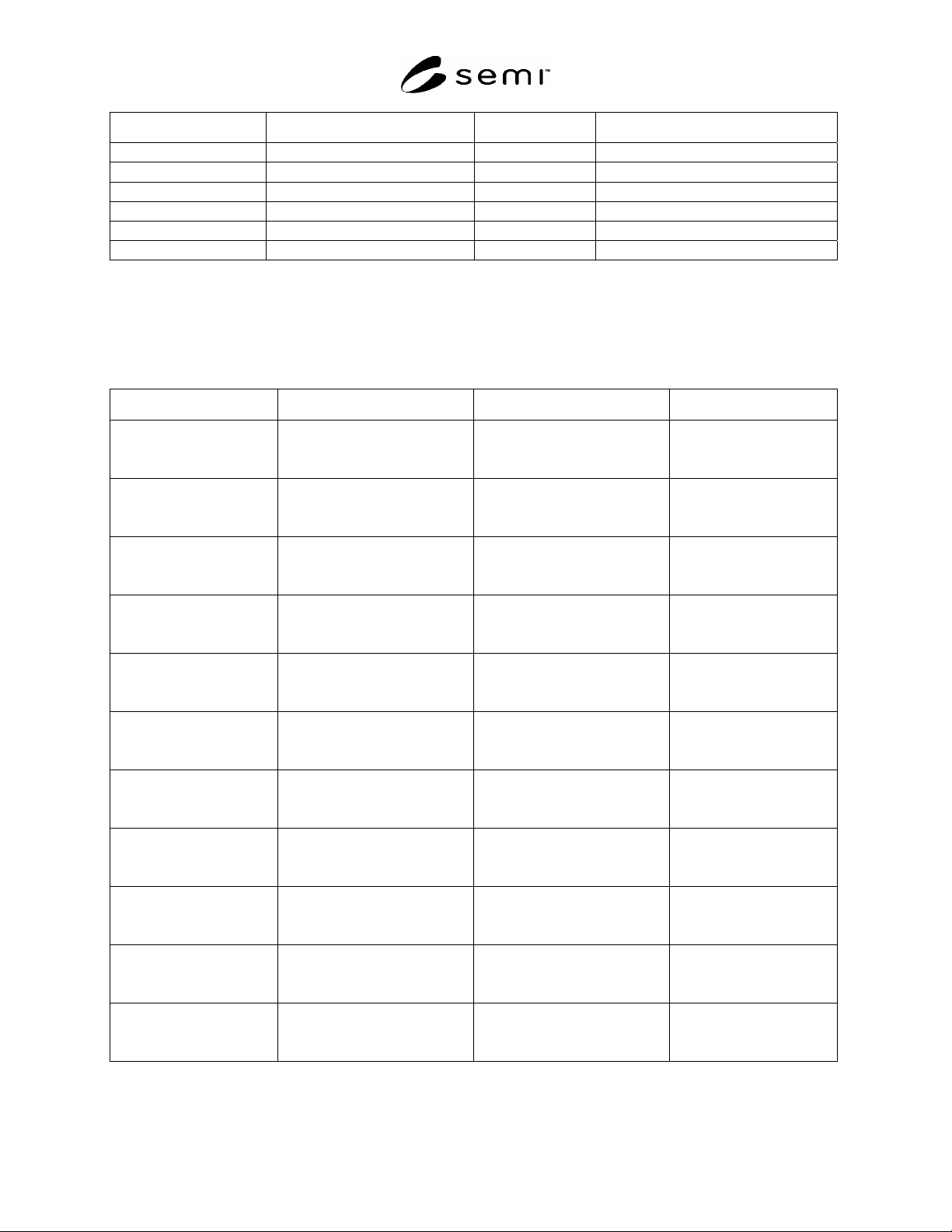
Service Message Name Supporting Class Stream, Function SECS-II Message Name
showData DieTraceData S14, F19/F20 Generic Service Request/Response
showDaughter CircuitModule S14, F19/F20 Generic Service Request/Response
showDTD DieTracer S14, F19/F20 Generic Service Request/Response
showPhenomena DieTraceClient S14, F19/F20 Generic Service Request/Response
showProperty CircuitModule, DieTraceData S14, F19/F20 Generic Service Request/Response
takeDTD DieTracer S14, F19/F20 Generic Service Request/Response
4.2 Service Parameter Mapping — The following table shows the mapping between service parameters defined by
SEMI T13 and data items defined by SEMI E5. The data item SVCNAME used with S14F19 is the text string
defined in the above table. The data item SPNAME used with S14F19/F20 is also text string defined in following
table. It is recommended but not limited to be case sensitive for both data items for future extension.
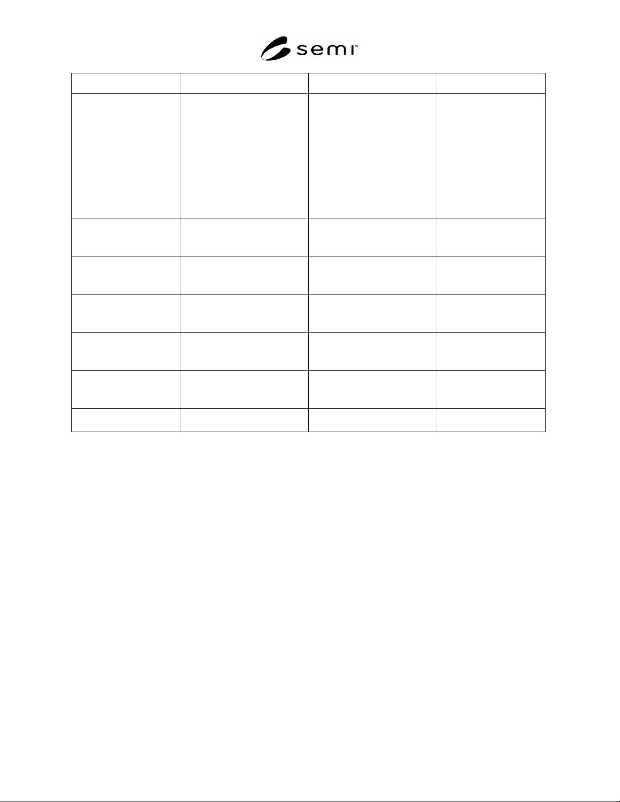
Table 2 Service Message Parameter Mapping
Parameter Name SECS-II Data Item Reference SECS-II Format Remarks
Alert L, 2
1. <SPNAME>
2. <SPVAL>
SPNAME = Alert
SPVAL = Item (00)
SPVAL: n-element list of
property item.
Clarifier L, 2
1. <SPNAME>
2. <SPVAL>
SPNAME = Clarifier
SPVAL = (20)
DataName L, 2
1. <SPNAME>
2. <SPVAL>
SPNAME = DataName
SPVAL = (20)
DataNameList L, 2
1. <SPNAME>
2. <SPVAL>
SPNAME = DataNameList
SPVAL = (20)
DataValue L, 2
1. <SPNAME>
2. <SPVAL>
SPNAME = DataValue
SPVAL = (00, 1x, 2x, 3x, 4x, 5x)
“x” is an appropriate octal
defined in SEMI E5.
Designation L, 2
1. <SPNAME>
2. <SPVAL>
SPNAME = Designation
SPVAL = (20)
If SPVAL is null or just
spaces, it means all. Spaces
could be separator.
Exceptions L, 2
1. <SPNAME>
2. <SPVAL>
SPNAME = Exceptions
SPVAL = Item (00)
SPVAL: n-element list of
property item.
MachineType L, 2
1. <SPNAME>
2. <SPVAL>
SPNAME = MachineType
SPVAL = (20)
ManagingTracer L, 2
1. <SPNAME>
2. <SPVAL>
SPNAME = ManagingTracer
SPVAL = (20)
Phenomena L, 2
1. <SPNAME>
2. <SPVAL>
SPNAME = Phenomena
SPVAL = Item (00)
SPVAL: n-element list of
property item.
Property L, 2
1. <SPNAME>
2. <SPVAL>
SPNAME = Property
SPVAL = Item (00)
SPVAL: n-element list of
property item.
SEMI T13.1-1104 © SEMI 2004 3
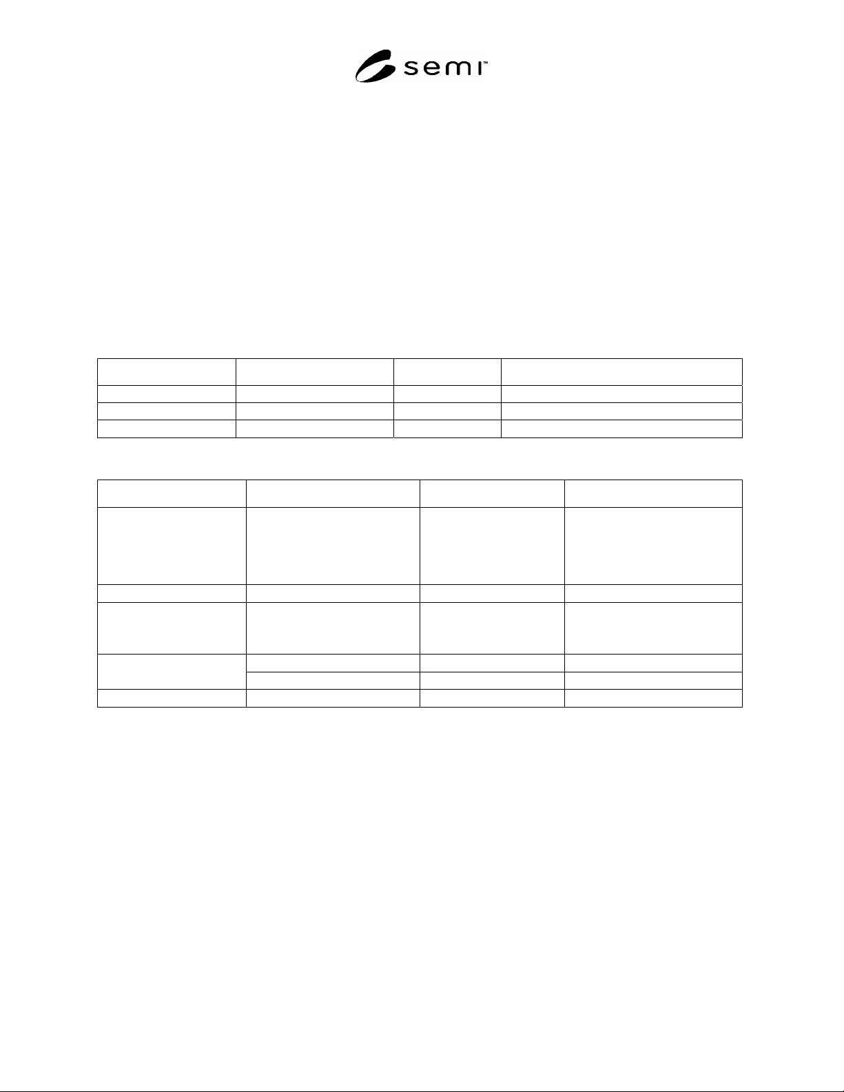
Parameter Name SECS-II Data Item Reference SECS-II Format Remarks
ServiceStatus L, 2
1. <SVCACK>
2. L, p
1. L, 2
1. <ERRCODE
1
>
2. <ERRTEXT
1
>
….. ….. …..
p. L, 2
1. <ERRCODE
p
>
2. <ERRTEXT
p
>
SVCACK = (10)
ERRCODE = (51, 52, 54)
ERRTEXT = (20)
If service was successful,
P = 0 and no error list is
attached.
If not, the maximum length
of each ERRTEXT must be
80.
Target L, 2
1. <SPNAME>
2. <SPVAL>
SPNAME = Target
SPVAL = (20)
TraceData L, 2
1. <SPNAME>
2. <SPVAL>
SPNAME = TraceData
SPVAL = (00, 1x, 2x, 3x, 4x, 5x)
“x” is an appropriate octal
defined in SEMI E5.
Tracer L, 2
1. <SPNAME>
2. <SPVAL>
SPNAME = Tracer
SPVAL = (20)
Tracers L, 2
1. <SPNAME>
2. <SPVAL>
SPNAME = Tracers
SPVAL = (20)
Item L, 2
1. <SPNAME>
2. <SPVAL>
PNAME = (20)
PVAL = (00, 20)
Name of Service <SVCNAME> 20 Note: message name other
than message parameter.
4.3 The Other Communication — The other SECS-II communication may additionally take place to run
manufacturing systems. Such communications as event report and exception notification are usually done from
equipment to host. Also some instructive communications for manufacturing as job management and remote
command are done from host to equipment. But they are just recommended to do regularly and independently to this
specification because they are not in the scope of traceability but in production scope.
SEMI T13.1-1104 © SEMI 2004 4
RELATED INFORMATION 1
SECS MAPPING FOR RESTRICTED INFORMATION
NOTICE: This related information is not an official part of SEMI T13.1 and was derived from the Japanese
Traceability Committee. This related information was approved for publication by full letter ballot on July 23,
2004.
R1-1 Particular Mapping for Specific Equipment
R1-1.1 Often some backend equipment may just handle such characteristic data of each device on a strip substrate
as sorting or classification data and transfer information. Characteristic information exchanging service messages
and their parameters are mapped as shown in the following tables. This mapping is one of possible specific
mappings for arrayed characteristic device information on a strip and there may not be a full mapping but just for
particular functions related to the exchanging services. This mapping is based on SEMI G84 with some extension.
Table R1-1 Service Instructions Mapping
Service Message Name Supporting Class Stream, Function SECS-II Message Name
showData DieTraceData S14, F1/F2 Get Attribute Request / Data.
ShowProperty DieTraceData S14, F1/F2 Get Attribute Request / Data.
takeDTD DieTracer S6, F11/F12 Selected Equipment Status Request / Data.
Table R1-2 Service Parameters Mapping
Parameter Name SECS-II Data Item Reference SECS-II Format Remarks
DataValue L, 2
1. <ATTRID>
2. <ATTRDATA>
ATTRID = (20)
ATTRDATA = (0, 1x, 2x,
3x, 4x, 5x)
showData of DieTraceData
(specific use for data content, or
whole characteristic map data on
a substrate including some
properties).
Designation <ATTRID> ATTRID = (20) showProperty of DieTraceData.
Property L, 2
1. <ATTRID>
2. <ATTRDATA>
ATTRID = (20)
ATTRDATA = (0, 1x, 2x,
3x, 4x, 5x)
showProperty of DieTraceData.
<ACKC6> ACKC6=(10) showData, showProperty. ServiceStatus
<OBJACK> OBJACK=(51) takeDTD of DieTracer.
TraceData <V> V=(0, 1x, 2x, 3x, 4x, 5x) takeDTD of DieTracer.
NOTICE: SEMI makes no warranties or representations as to the suitability of the standards set forth herein for any
particular application. The determination of the suitability of the standard is solely the responsibility of the user.
Users are cautioned to refer to manufacturer's instructions, product labels, product data sheets, and other relevant
literature, respecting any materials or equipment mentioned herein. These standards are subject to change without
notice.
By publication of this standard, Semiconductor Equipment and Materials International (SEMI) takes no position
respecting the validity of any patent rights or copyrights asserted in connection with any items mentioned in this
standard. Users of this standard are expressly advised that determination of any such patent rights or copyrights, and
the risk of infringement of such rights are entirely their own responsibility.
Copyright by SEMI® (Semiconductor Equipment and Materials
International), 3081 Zanker Road, San Jose, CA 95134. Reproduction of
the contents in whole or in part is forbidden without express written
consent of SEMI.