semi合集-English.pdf - 第975页
SEMI E129-1103 © SEMI 2003 13 A1-2.7 Guide Reco mmendations A1-2.7.1 This document recomm ends the values shown in pare ntheses in the second colum n of Table A1-8 of this Appe ndix and includes them in Section 12.5 Tabl…
SEMI E129-1103 © SEMI 2003 12
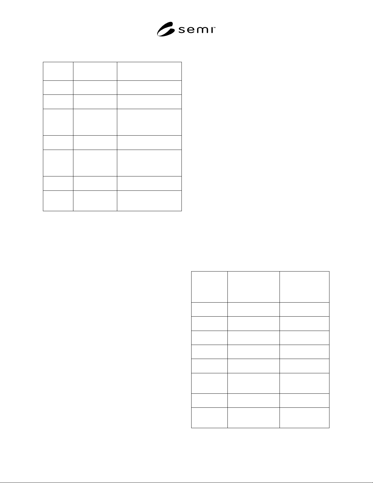
Table A1-7 Electrostatic Field Levels – Limit Particle
Deposition in a Class 1 Environment
Year
Node
N/A,
defects/cm
2
Electrostatic Field, V/cm
2000
180 nm
0.0141 180
2002
130 nm
0.0093 120
2003
100 nm
(2004)
(90 nm)
0.0089 114
2007
65 nm
0.0059 75
2009
50 nm
(2010)
(45 nm)
0.0056 71
2012
32 nm
0.0043 55
2015
25 nm
(22 nm)
0.0044 56
A1-2.6.3 A second problem for semiconductor
manufacturing occurs in the presence of a changing
electric field. This occurs when there is movement of
isolated conductors within an electric field, or the field
itself changes in magnitude. The result is that the
charge, and hence the voltage, induced on the
individual isolated conductors will not always be the
same, creating a potential difference between the
conductors. Under the right circumstances, ESD events
can occur between conductors at different potentials.
With the electric field changing, there is also the
likelihood that multiple ESD events will occur.
A1-2.6.4 This phenomenon of charge induced by
changing electric fields is mostly a concern in the
handling of photomasks with µm and sub-micron
feature sizes. While ESD damage occurred with 5×
photomasks with 3 to 5-µm features, it was infrequent.
At the 180-nm technology node, even 5× masks have
sub-micron features and the trend is to 4× masks,
making the feature sizes even smaller.
A1-2.6.5 The problem occurs because a photomask is
basically a large collection of closely spaced, isolated
conductors on an insulating quartz substrate. The
substrate is easily charged, creating an electric field.
The field changes whenever the spacing between the
photomask and ground changes (e.g., during handling
by robotics). Transporting the photomask, whether in
static dissipative reticle carriers or not, exposes it to
changing electric fields from other charged objects
(e.g., equipment panels, windows, work surfaces, and
equipment parts). The result is an increasing incidence
of ESD damaged photomasks as geometries shrink.
A1-2.6.6 While there have been several studies
documenting the existence of the field charging
problem on photomasks, there is currently a need for
further research to demonstrate the level at which it
occurs for production facilities. A recent study
(Montoya, et al.) was able to produce the following
information:
1. Testing was done on a photomask test device with
1.5-µm gaps between features. Approximately 800
V/cm (2 kV/inch) of electric field was needed to
cause damage.
2. Current production 180-nm photomasks are 4×
with a nominal gap width of 0.72 µm (or less
depending on the technology). ESD should occur
at 400 V/cm (1 kV/inch) or less.
3. To avoid ESD on 180-nm photomasks, electric
fields should be kept below 50% of the damage
threshold, or 200 V/cm (500 V/inch).
A1-2.6.7 Table A1-8 below is based on these
measurements. It is acknowledged that discharge
phenomena may change at very small conductor
spacing, and that the relationship to electric field may
not be a linear function of the geometry. The values in
Table A1-8 may need to be changed as more
information becomes available.
Table A1-8 Electrostatic Field Levels – Limit Induced
ESD Damage on Photomasks
Year
Node
Electrostatic Field
Limits
Induced ESD Damage,
V/cm
Electrostatic Field
Limits
Particle Attraction,
V/cm
2000
180 nm
200 (200) 180
2002
130 nm
144 (150) 120
2003
100 nm
111 (125) 114
2004
90 nm
100 (100) 114
2007
65 nm
72 (70) 75
2009
50 nm
(45 nm)
55 (50) 71
2012
32 nm
35 (35) 55
2015
25 nm
(22 nm)
27 (25) 56

SEMI E129-1103 © SEMI 2003 13
A1-2.7 Guide Recommendations
A1-2.7.1 This document recommends the values
shown in parentheses in the second column of Table
A1-8 of this Appendix and includes them in Section
12.5 Table 1.
A1-2.8 Guide Recommendations for Equipment
Malfunctions
A1-2.8.1 Most semiconductor manufacturing
equipment should comply with the ESD immunity
requirements of the European Economic Community
(EEC). The testing mandated by the EEC uses the test
methods and ESD immunity levels specified in IEC/TS
61000-4-2. To test for compliance, measurements are
made with an ESD simulator described by IEC/TS
61000-4-2. Equipment is required to pass a test
involving the discharge produced by a 150-pF capacitor
charged to 4000 V, or 600 nC.
A1-2.8.2 Users should note that the above test
discharge level and properties (i.e. discharge voltage,
discharge model and pulse rise time) may not be
sufficient to predict actual discharges that occur in
semiconductor production environments. In addition,
the ESD immunity of equipment in an isolated test
environment may change when it is installed in a
production environment.
A1-2.8.3 The discharge test specified in IEC/TS
61000-4-2 is done at significantly higher charge levels
than are recommended for objects in the facility in
Table A1-2 of this Appendix. If the recommendations
of Table A1-2 are followed, static charge levels should
be low enough to prevent ESD-induced equipment
malfunctions.
A1-2.8.4 If the recommended electrostatic levels
regarding ESD contained in Section 12.5 Table 1 are
not used, those contained in SEMI E78 should be used
for equipment.
A1-3 References
SEMI E78 — Electrostatic Compatibility
– Guide to
Assess and Control Electrostatic Discharge (ESD) and
Electrostatic Attraction (ESA) for Equipment
Montoya, J. A., Levit, L., and Englisch, A., “A Study of
the Mechanisms of ESD Damage for Reticles”,
Electrical Overstress/Electrostatic Discharge
Symposium Proceedings, 394-405 (2000)
Cooper, D. W., Miller, R. J., Wu, J. J., and Peters, M.
H., "Deposition of Submicron Aerosol Particles During
Integrated Circuit Manufacturing: Theory", Particulate
Sci. Technol. 8 (3 and 4): 209-224 (1990)
Liu, B. Y. H., and Ahn, K. H., "Particle Deposition on
Semiconductor Wafers", Aerosol Sci. Technol. 6: 215 -
224 (1987)
International Technology Roadmap for Semiconductors
(1999, 2002, 2003)
8
ISO 14644 – Cleanrooms and Associated Controlled
Environments – Part 1 – Classification of Air
Cleanliness
9
NOTICE: SEMI makes no warranties or
representations as to the suitability of the standards set
forth herein for any particular application. The
determination of the suitability of the standard is solely
the responsibility of the user. Users are cautioned to
refer to manufacturer’s instructions, product labels,
product data sheets, and other relevant literature
respecting any materials mentioned herein. These
standards are subject to change without notice.
The user’s attention is called to the possibility that
compliance with this standard may require use of
copyrighted material or of an invention covered by
patent rights. By publication of this standard, SEMI
takes no position respecting the validity of any patent
rights or copyrights asserted in connection with any
item mentioned in this standard. Users of this standard
are expressly advised that determination of any such
patent rights or copyrights, and the risk of infringement
of such rights, are entirely their own responsibility.
8 International SEMATECH, 2706 Montopolis Drive, Austin, TX
78741, USA (www.sematech.org)
9 Institute of Environmental Sciences and Technology (IEST), 5005
Newport Drive, Rolling Meadows, IL, 60008-38411, USA
(www.iest.org)

SEMI E129-1103 © SEMI 2003 14
RELATED INFORMATION 1
DEVICE SENSITIVITY MEASUREMENTS
NOTICE: The material contained in this related information is not an official part of SEMI E129 and is not
intended to modify or supersede the guide in any way. These notes are provided as a source of information to aid in
the application of the guide, and are to be considered reference material. Determination of the suitability of the
material is solely the responsibility of the user. This related information was approved by full letter ballot
procedures on September 3, 2003.
R1-1 ESD Damage
R1-1.1 Introduction
R1-1.1.1 ESD damage to devices occurs when they
come into contact with personnel and facility or
equipment surfaces. Either may store a residual charge
large enough to destroy the device if a discharge occurs.
It is also possible that charge stored on insulating parts
of products or reticles will induce charges on their
conductive parts. Discharges may occur between
conductive parts at different potentials or when the
conductive parts touch ground. The same types of
induced charge can be produced when products or
reticles are placed in the electrostatic field produced by
static charge on facility or equipment surfaces that are
insulative or isolated from ground. In the
semiconductor industry, it has been established that
significant proportions of customer field returns are
attributed to damage resulting from ESD.
R1-1.2 Description of ESD Damage Mechanisms
R1-1.2.1 ESD failures are the result of either a current-
induced phenomenon or a charge-induced phenomenon,
and the damage can either be junction, contact,
dielectric or oxide related. The apparent similarity in
current-induced damage resulting from ESD due to
human body model (HBM) discharges or machine
model (MM) discharges results from the thermal nature
of both of these processes. The HBM and MM
damages result when the temperature (joule heating) of
the region dissipating the ESD pulse energy reaches a
critical value and melting occurs.
R1-1.2.2 The charged device model (CDM) predicts
charge-induced phenomena. For CDM-type discharges,
oxide punch through occurs when the ESD voltage
applied across the oxide creates a high enough field to
break down the oxide. Excessive current flow results,
causing an oxide short, but there is no heat transfer
(adiabatic process). It should be noted here that the
time duration for typical ESD events from charged
objects and personnel ranges from 10 to 100 ns, while
CDM-type events occur in less than 1 ns.
R1-1.3 Device Testing Models
R1-1.3.1 Human Body Model (HBM) — The HBM is
the oldest and the most widely used of the three ESD
models. The model attempts to replicate the discharge
when a charged human touches a device that is at a
lower potential. Human capacitance and resistance
have been chosen to be 100 pF and 1500 Ω
respectively. The values were chosen after
measurements were made on humans in varying
positions with respect to their surroundings. The
resulting discharge waveform has a double exponential
shape with rise time range of 2–10 ns and a decay
constant (1/e position) of 150 ± 20 ns. The typical peak
currents range from 0.67 A at 1000 V to 2.67 A at 4000
V.
R1-1.3.2 Machine Model (MM) — The MM is
described by the Electronic Industries Association of
Japan (EIAJ) as a worst-case HBM. The model
attempts to replicate the discharge from a metallic arm
of an automatic handler coming into contact with the
metallic leads of a semiconductor device. A
capacitance of 200 pF and ideally zero resistance
produces a sinusoidal decaying waveform with an
effective pulse duration of 200 ns. The typical peak
currents range from 1.75 A at 100 V to 14.0 A at 800 V.
Note that MM failures occur at 5–10 times lower
voltage than HBM.
R1-1.3.3 Charged Device Model (CDM) — The CDM
in its purest form is actually a field-induced model
because the device is actually part of model. This
model attempts to describe a device which itself
becomes charged due to an external field, or due to
triboelectric charging of the device surfaces. During
discharge the parasitics (i.e., capacitance, inductance
and impedance) in the device play a significant role in
the resulting failure. The discharge pulse is a sinusoidal
waveform with an extremely fast rise time of less than
500 ps. The waveform decays rapidly with a total pulse
duration of less than 5 ns. The peak currents range
from 2.0 A at 250 V charging voltage to 18.0 A at 2000
V charging voltage.
R1-1.3.4 Correlation Between Models — Whether or
not a correlation exists between HBM and MM is
debatable. While some companies report a correlation