semi合集-English.pdf - 第7276页
SEMI MF928-0305 © SEMI 2005 2 3 Limitations 3.1 In Method B, the profile of the para llel surfa ces of the wafer may not be sharply focused at distances exceeding approxim ately 0.5 mm (0.02 0 in.) from th e extreme wafe…
SEMI MF928-0305 © SEMI 2005 1
SEMI MF928-0305
TEST METHODS FOR EDGE CONTOUR OF CIRCULAR
SEMICONDUCTOR WAFERS AND RIGID DISK SUBSTRATES
These test methods were technically approved by the Global Silicon Wafer Committee and are the direct
responsibility of the North American Silicon Wafer Committee. Current edition approved for publication by
the North American Regional Standards Committee on December 10, 2004 Initially available at
www.semi.org January 2005; to be published March 2005. Original edition published by ASTM
International as ASTM F 928-85. Last previous edition SEMI MF928-02.
1 Purpose
1.1 The edges of circular wafers of electronic materials are frequently required to be shaped after cutting the wafers
from the ingot. Contouring the wafer edge reduces the incidence of chipping and minimizes epitaxial edge crown
and photoresist edge bead during subsequent processing of the wafer. Similarly, edges of rigid disk substrates are
frequently edge shaped.
1.2 The test methods described here provide means to determine that the wafer edge contour is appropriate to meet
specifications, such as SEMI M1 or SEMI M9, which are intended to provide wafers avoiding the difficulties
enumerated above.
2 Scope
2.1 These test methods provide means for examining the edge contour of circular wafers of silicon, gallium
arsenide, and other electronic materials, and determining fit to limits of contour specified by a template that defines
a permitted zone through which the contour must pass. Principal application of such a template is intended for, but
not limited to, wafers that have been deliberately edge shaped.
NOTE 1: DIN 50441/2 is equivalent to Method B of this standard. It is the responsibility of DIN Committee NMP 221. DIN
50441/2, Measurement of the Geometric Dimensions of Semiconductor Slices; Testing of Edge Rounding, is available from
Beuth Verlag GmbH, Burggrafenstrasse 6, 10787 Berlin, Germany, Telephone: 49.30.2601-0, Fax: 49.30.2601.1263, Website:
www.beuth.de.
2.2 Two test methods are described.
2.2.1 Method A is destructive and is limited to inspection of discrete points on the periphery, including flats. The
contour of deliberately edge-shaped wafers may not be uniform around the entire periphery, and thus the discrete
location(s) may or may not be representative of the entire periphery.
2.2.2 Method A is recommended for examining the edge profile of flatted regions of the wafer.
2.2.3 Method A is best suited for referee purposes.
2.3 Method B is nondestructive and suitable for inspection of all points on the wafer periphery except flats.
2.3.1 Method B is appropriate for routine process monitoring such as alignment of wafer edge grinders, routine
quality control and incoming/outgoing inspection purposes. In view of the uncertainty of precisely locating the
intersection of the contour and the wafer surface when carrying out Method B, use of this method for commercial
transactions is not recommended unless the parties to the test establish the degree of correlation that can be obtained.
2.3.2 Method B may also be applied to the examination of the edge contour of the outer periphery of substrates for
rigid disks used for magnetic storage of data; metallic rigid disk substrates cannot conveniently be cleaved.
NOTE 2: Reference to wafers in the remainder of this standard shall be interpreted to include substrates for rigid disks unless the
phrase “of electronic materials” is also included in the context.
2.4 The values stated in SI units are to be regarded as the standard. The values given in parentheses are for
information only.
NOTICE: This standard does not purport to address safety issues, if any, associated with its use. It is the
responsibility of the user of this standard to establish appropriate safety and health guides and determine the
applicability of regulatory or other limitations prior to use.

SEMI MF928-0305 © SEMI 2005 2
3 Limitations
3.1 In Method B, the profile of the parallel surfaces of the wafer may not be sharply focused at distances exceeding
approximately 0.5 mm (0.020 in.) from the extreme wafer edge toward the wafer center. This uncertainty in the
wafer surface location may cause inaccuracy in positioning the wafer with respect to template lines. It may also
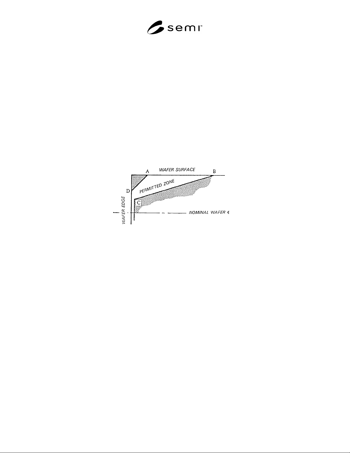
make it difficult to determine whether the wafer edge profile lies within the permitted zone at point B of the
template (see Figure 1). These difficulties can be overcome by aligning a straight edge to the wafer surface by direct
contact, observing the shadow extension in the sharply focused region, and extrapolating the straight line edge of the
template reference. In applying this technique, exercise care to avoid damaging or contaminating the wafer surface.
3.1.1 This limitation renders Method B unsuitable for determining the distance between the front and back wafer
surfaces. The edge contours near the front and back surfaces of the wafer must be inspected separately.
3.2 In Method B, attempting to view the complete wafer periphery, except flats, through wafer rotation may
necessitate frequent focus adjustment due to variations in wafer roundness and fixturing precision, including wafer
centering.
3.3 By either test method, any foreign material such as large particles or high spots on the wafer surface in the light
path will present a false edge contour by masking the true contour shape.
3.4 It is not always feasible to provide a uniform radius or bevel to the edges of wafers because silicon, gallium
arsenide, and many other electronic materials as well as glass disk substrates are both hard and brittle. Wear of
grinding tools, process variations, and the presence of flats on the circumference of wafers cause practical contours
to have varying shapes. For this reason, templates are used that define an allowed range.
3.5 If a television system is used, the user is cautioned that distortions in the horizontal and vertical deflections may
occur (see ¶9.2).
4 Referenced Standards
4.1 SEMI Standards
SEMI M1 — Specifications for Polished Monocrystalline Silicon Wafers
SEMI M9 — Specifications for Polished Monocrystalline Gallium Arsenide Slices
4.2 ANSI Standard
1
ANSI/ASQC Z1.4 — Sampling Procedures and Tables for Inspection by Attributes
NOTICE: Unless otherwise indicated, all documents cited shall be the latest published versions.
5 Summary of Test Methods
5.1 Both test methods employ optical means to project a shadow of the edge contour at substantial magnification on
a screen.
5.1.1 In applying Method A (destructive) the sample wafer is cleaved or broken along a diameter. A sharply
focused image of the cross section of the wafer is obtained over a sufficiently large region near the edge with the aid
of an optical comparator or projection microscope.
5.1.2 In Method B (nondestructive) the unbroken wafer is back lighted with collimated (parallel) light such that a
sharply defined shadow of the wafer edge is projected on a screen. In this test method the wafer is not altered in any
way.
5.2 By either test method, the contour of the wafer edge profile image is compared to a template that has been
mounted or projected on the screen. The template defines a permitted zone through which the edge contour must
pass.
1 American National Standards Institute, New York Office: 25 West 43rd Street, New York, NY 10036, USA. Telephone: 212.642.4900, Fax:
212.398.0023, Website:
www.ansi.org
.
SEMI MF928-0305 © SEMI 2005 3
6 Apparatus
6.1 For Method A, an optical comparator or projection microscope capable of 100× magnification with viewing
screen large enough to permit display of an area 1 mm by 1 mm (0.04 in. by 0.04 in.).
6.2 For Method B, a collimated light source (coherent or incoherent) and a television system, consisting of a
camera, lenses to give 100× magnification and TV monitor capable of displaying a 1 by 1 mm (0.04 by 0.04 in.)
area.
NOTE 3: An adjustable camera mount, slice holding fixture, or lens adjustment is desirable for sharp focusing.
6.3 Fixture, for holding the wafer to be tested. The fixture must provide means for positioning the wafer such that
the plane of the surface of the wafer is parallel to the viewing direction. The fixture should be arranged in such a
way that its position and orientation in a plane perpendicular to the viewing direction can be adjusted conveniently,
or alternatively, the template can be moved. Optionally, for Method B, the fixture can provide means for rotation of
the wafer about its axis of symmetry. The design of the fixture for Method B should be such that the wafer may be
loaded, held in position, and unloaded with minimum risk of contamination or damage to the wafer.
6.4 Template, having transparent regions defining the area through which the contour of the edge of the wafer must
pass and a semi-transparent region bounding the space. An example of a template is given in Figure 1. Instructions
for constructing templates are given in §10.
NOTE: Only half is used to emphasize that these methods are not intended for measurement of thickness.
Figure 1
Template Showing One Half of Wafer Cross Section
6.5 Gage Block or Precision Rod, with dimensions approximately the same as the thickness of the wafer to be
tested and accurately known for use in establishing the magnification of the apparatus.
6.6 Rule, 150 mm (6 in.) long with scale gradations of 0.5 mm (0.02 in.) or less.
7 Sampling
7.1 Unless otherwise specified, ANSI/ASQC Z1.4 shall be used. Inspection levels shall be agreed upon between
the supplier and purchaser.
7.2 The number and location of the test points on the periphery of each wafer shall be agreed upon between the
supplier and purchaser.
8 Specimen Preparation
8.1 For Method A, cleave or fracture the wafer along a diameter.
NOTE 4: This may be conveniently accomplished by positioning the wafer over a small diameter rod and pressing downward on
both sides. Alignment by eye is sufficient. If required by the sampling plan, cleave additional pieces along the edge of the wafer.
9 Determination of Magnification Factor
9.1 For Method A, adjust the comparator or microscope to the magnification to be used for the test. Using a gage
block or precision rod of accurately known dimensions, follow the comparator or microscope manufacturer's
instructions to establish object-to-image magnification to three significant figures.