semi合集-English.pdf - 第7841页
SEMI T13-1104 © SEMI 2004 1 SEMI T13-1104 SPECIFICATION FOR DEVICE TR ACKING: CONCEPTS, BEHAVIOR AND SERVICES This specificati on was technically approved by the Global Trac eability Committee and is the direct responsib…
SEMI T12.2-0704 © SEMI 2004 69
Client
(H TT P Cli ent)
Br oker
(H TT P Se r ver )
HTTP POST <M essageC1>
HTT P 200 <A cknowledge>
Cl ient
(H T TP Cl i ent )
Broker
(H TT P Ser ve r )
H T T P POST <get M essag e>
HTT P 200 <MessageB1>
Cl ient
(HTTP Client)
Br ok er
(H TTP Ser ve r )
H TTP POST <g et Me ssage >
HTT P 200 <empt y>
H TTP POST <A ck nowledge>
HT TP 200 <empt y>
Cl ient
(H TT P Cli ent)
Br ok er
(H TT P Ser ve r )
H TTP POST <M essa geC2 >
H TTP 200 <A cknowledge>
Cl ient
(HTTP Client )
HTTP POST <get Message>
HTTP 200 <MessageC2>
HTTP POST <A cknowledge>
HT TP 200 <empt y>
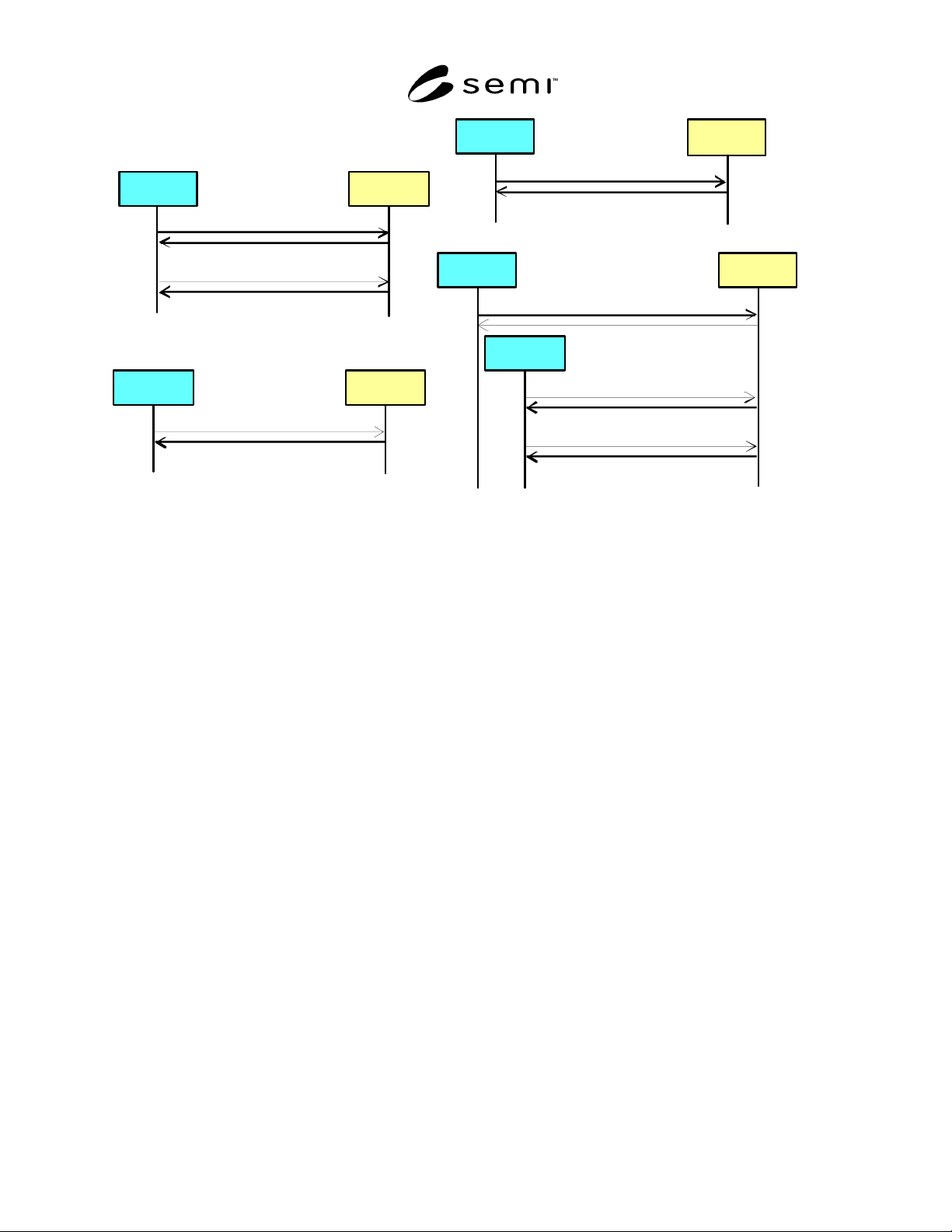
Message f r om Client t o Br oker
Message f rom Broker t o Client
No Message f rom Broker to Client
Message between Clients
Figure R1-2
Communication with Message Broker
NOTICE: SEMI makes no warranties or representations as to the suitability of the standards set forth herein for any
particular application. The determination of the suitability of the standard is solely the responsibility of the user.
Users are cautioned to refer to manufacturer' s instructions, product labels, product data sheets, and other relevant
literature, respecting any materials or equipment mentioned herein. These standards are subject to change without
notice.
By publication of this standard, Semiconductor Equipment and Materials International (SEMI) takes no position
respecting the validity of any patent rights or copyrights asserted in connection with any items mentioned in this
standard. Users of this standard are expressly advised that determination of any such patent rights or copyrights, and
the risk of infringement of such rights are entirely their own responsibility.
Copyright by SEMI® (Semiconductor Equipment and Materials
International), 3081 Zanker Road, San Jose, CA 95134. Reproduction o
f
the contents in whole or in part is forbidden without express written
consent of SEMI.

SEMI T13-1104 © SEMI 2004 1
SEMI T13-1104
SPECIFICATION FOR DEVICE TRACKING: CONCEPTS, BEHAVIOR
AND SERVICES
This specification was technically approved by the Global Traceability Committee and is the direct
responsibility of the Japanese Traceability Committee. Current edition approved by the Japanese Regional
Standards Committee on April 30, 2004. Initially available at www.semi.org June 2004; to be published June
2004.
NOTICE: The designation of SEMI T13 was updated during the 1104 publishing cycle to reflect the creation of
SEMI T13.1 and SEMI T13.2.
1 Purpose
1.1 The purpose of this specification is to trace devices
for the sake of quality control, warranty, security or
any other reasons. This specification makes it easy to
transfer information required for realizing tracing in
such semiconductor products as dice and packaged
devices.
1.2 Because modern market trend of consumer minds,
industries and governments are explicitly or implicitly
requiring traceability for all products including
semiconductor devices. Implementing this specification
will help to satisfy both direct and indirect consumers
of semiconductor devices.
1.3 The other purpose of this document is to clarify
means to define coordinates to specify physical
position of devices on substrates which the other
standard documents don’t address. This information is
provided in Appendix sections.
2 Scope
2.1 This specification is intended to realize
semiconductor device tracking rather than production
itself. Even if some operations or communications for
tracing purpose may be related to factory automation or
production including measurement and maintenance,
they are not in the scope of this specification but
references to work within a factory.
2.2 Because the object of this specification is
traceability, tracing dice is not bounded on packaging
process of semiconductor devices. For example bare
dice may be mounted on Print Circuit Board (PCB).
This specification describes not only what is required
to trace dice in semiconductor manufacturing fab but
also what could be shared in PCB assembly lines or set
makers.
2.3 This document describes device tracking data
transfer between entities in a fab. Some entities may be
physical or logical depending on configuration of the
fab. Sometimes the transfer is carried out between
entities in different companies over such
communication media as internet or VPN (Virtual
Private Network). While this document describes the
transferring interface, it doesn’t define security
specification or criteria to be used with this
specification.
2.4 This document describes tracking semiconductor
devices. To make it possible to track final assembled
products of semiconductor devices consistently, this
document describes such assembled materials. Also,
sometimes a semiconductor device may consist of
more than one die. To track the smallest unit this
document often uses “Die Tracking” or “Die Tracing”
rather than “Device Tracking.”
NOTICE: This standard does not purport to address
safety issues, if any, associated with its use. It is the
responsibility of the users of this standard to establish
appropriate safety and health practices and determine
the applicability of regulatory or other limitations prior
to use.
3 Limitations
3.1 While this specification could be effective in such
industry as PCB assembly, it is not required to comply
with this specification. Semiconductor device
producers who implement this specification will find
communicating die trace information with later
assembly manufacturers easier and more effective if
they comply this specification. The reverse is also true.
3.2 Because this specification doesn’t talk about
security considerations, implementers of this
specification are required realizing security data
transfer or connection with foreign computers. It is the
responsibility of the readers of this document to discuss
this issue between users and suppliers.
3.3 This document specifies logical information
definitions and related message exchanges required for
die trace systems, and assumes that any process or
equipment verifies passed material or product by any
means. This document doesn’t specify how it is done,
which ID tags and readers are recommended or where
and when it must be done. However target equipment
and production systems have to make sure the

SEMI T13-1104 © SEMI 2004 2
verification occurs. Even if some physical
identification may be difficult to verify because
something is hidden by the other material or no
physical identification tag is provided, they have to
cover by some means.
3.4 Tracking die coordinate information on substrates
is a subset of full device tracking. Readers who have
just interested in die coordinate information (narrow
Device Tracking) can skip most sections and go
straight to Appendix and Related Information sections
to implement the specification.
4 Referenced Standards
4.1 SEMI Standards
SEMI E130 — Specification for Prober Specific
Equipment Model for 300 mm Environment
(PSEM300)
SEMI G81 — Specification for Map Data Items
SEMI G84 — Specification for Strip Map Protocol
SEMI G85 — Specification for Map Data Format
SEMI M17 — Guide for Universal Wafer Grid
SEMI M20 — Specification for Establishing a Wafer
Coordinate System
SEMI M21 — Specification for Assigning Addresses
to Rectangular Elements in a Cartesian Array
4.2 The Internet Engineering Task Force
1
RFC2396 — Uniform Resource Identifiers (URI):
Generic Syntax
NOTICE: Unless otherwise indicated, all documents
cited shall be the latest published versions.
5 Terminology
5.1 Abbreviations & Acronyms
5.1.1 PCB — Print Circuit Board
5.1.2 SMT — Surface Mount Technology
5.1.3 SMTP — Simple Mail Transfer Protocol
5.1.4 SIP — System In Package
5.2 Definitions
5.2.1 cabinet — a kind of enclosure for electronics to
keep from exposure of electrodes and/or
subcomponents, and/or to give some means of human
operation.
5.2.2 cassette — a kind of container of electronics
materials or parts for the purpose of carrying
1 The Internet Engineering Task Force;
www.ietf.org,
capability, grouping operation, replaceability at
inlet/outlet port or similar objectives.
5.2.3 circuit module — an implemented electric circuit
with active/passive elements in a cell, on a substrate or
packaged together.
5.2.4 device — a concise representation of a
semiconductor device. It must be a semiconductor die
regardless whether it is on the way of fabrication or
completed, whether it has been diced or not, whether it
is installed/mounted on some substrate or not, or
whether it is packaged or not. If it is packaged, the
whole package is assumed as a device and a device
may have more than one dice. In some specific case a
device may have some other active or passive elements
in the package.
5.2.5 Device Tracking — generic term of Die Trace
regardless of unit of tracing or category of information.
Following narrow sense is also applied in some specific
fields. A specific case of tracking especially for
geometric coordinates information on holding
substrate. Because sometimes this specific type of
Device Tracing information is very convenient to such
end user industries as the automobile or car parts
industries, this is defined separately. This can be
realized with limited specification presented in
Appendix sections of this specification.
5.2.6 dicing frame — a frame with sticky plastic film
to mount a semiconductor wafer for dicing.
5.2.7 die — a semiconductor product which has
electric elements and wiring. Many dice are usually
fabricated on a semiconductor substrate at a time which
is often referred to as wafer and the substrate is diced
for dice before packaging or mounting on some other
substrate. Some die may be fabricated on such isolator
as thin transparent glass plate. Die is intended as it is
just one piece of substrate even if it is packaged with
the other dice.
5.2.8 Die Trace — acquiring die information for
tracing the die and/or processing the information to
investigate what happens on the die during
manufacturing or to ensure such properties of the die as
producer and facilities. The information for such
aggregating entities as wafer and PCB may be included
depending on the usefulness of the information for
tracing because they are produced with the die on them.
5.2.9 glass plate — a rectangular thin insulator plate to
fabricate one or more electric elements on it. Often the
material of this plate is transparent glass for flat panel
display, sometimes it may be ceramic for passive
electric elements. The purpose of definition of this item
is just to introduce one of possible examples to trace
and this document doesn’t specify details.