semi合集-English.pdf - 第6526页
SEMI G81-0703 © SEMI 2000, 2003 1 SEMI G81-0703 SPECIFICATION FOR MAP DATA I TEMS This specification was technically approved by the Gl obal Auto mated Test Equipm ent Committee and is the direct responsibility of the No…
SEMI G80-0200 © SEMI 200033
A4.4 Use of a Loop-Through Sampling Head
A4-4.1 This is an alternate approach to measured RMS
signal jitter. The input signal is routed through the loop-
through sampling head where it is sampled and sent to
the output of the sampling head. The head output is
connected to the oscilloscope trigger. (See Figure A4-
3.)
A4-4.2 What is Observed When Making MS And MI
Measurements — This dialog is meant to provide
further clarification for making jitter measurements.
This is an example that applies to a jitter measurement
using an oscilloscope with an inherent oscilloscope
delay of 20ns. The signal frequency is 100MHz (period
of 10ns ). The semi-rigid coax delay is set to the
inherent oscilloscope delay of 20ns.
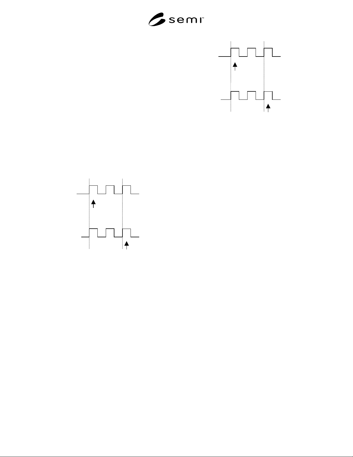
A4-4.3 Measured RMS Signal Jitter, MS — For the
MS measurement the observed edge occurs subsequent
to the edge that triggered the oscilloscope:
N
N
+1
N
+2
N
+2
This pulse triggers the oscilloscope.
Observed Edge –– The pulse that is
displayed on the oscilloscope is not the
same pulse that triggered the oscilloscope.
Trigger:
Signal:
Figure A4-4
Measured RMS Signal Jitter, MS
A4-4.4 The observed edge depends upon the signal
frequency; thus what is displayed is subsequent to the
trigger pulse permitting signal jitter to be observed.
A4-4.5 Measured RMS Instrumentation Jitter, MI —
For the MI measurement the observed edge is the same
edge that triggered the oscilloscope.
N
–1
N
+1
N
+2
N
This pulse triggers the oscilloscope.
Observed Edge –– The pulse that is
displayed on the oscilloscope is the same
pulse that triggered the oscilloscope.
N
–2
Trigger:
Signal:
Figure A4-5
Measured RMS Instrumentation Jitter, MI
A4-4.6 There is no repetitive aspect of the signal, thus
whatever jitter you observe is strictly instrumentation
jitter.
A4-4.7 Summary –– Jitter is only observable for a
periodic signal or repetitive edge. Thus when MS
measurements are made signal jitter is observed
because a subsequent or repetitive signal is displayed
(in addition to instrumentation jitter). When MI
measurements are made the input signal is delayed such
that you see the same edge that trigger the oscilloscope.
That creates a non-repetitive or non-periodic occurrence
of the observed signal, thus the jitter observed is strictly
due to the instrumentation.
NOTICE: SEMI makes no warranties or
representations as to the suitability of the standards set
forth herein for any particular application. The
determination of the suitability of the standard is solely
the responsibility of the user. Users are cautioned to
refer to manufacturer’s instructions, product labels,
product data sheets, and other relevant literature
respecting any materials mentioned herein. These
standards are subject to change without notice.
The user’s attention is called to the possibility that
compliance with this standard may require use of
copyrighted material or of an invention covered by
patent rights. By publication of this standard, SEMI
takes no position respecting the validity of any patent
rights or copyrights asserted in connection with any
item mentioned in this standard. Users of this standard
are expressly advised that determination of any such
patent rights or copyrights, and the risk of infringement
of such rights, are entirely their own responsibility.
Copyright by SEMI® (Semiconductor Equipment and Materials
International), 3081 Zanker Road, San Jose, CA 95134. Reproduction o
f
the contents in whole or in part is forbidden without express written
consent of SEMI.

SEMI G81-0703 © SEMI 2000, 2003 1
SEMI G81-0703
SPECIFICATION FOR MAP DATA ITEMS
This specification was technically approved by the Global Automated Test Equipment Committee and is the
direct responsibility of the North American Automated Test Equipment Committee. Current edition approved
by the North American Regional Standards Committee on March 12, 2003. Initially available at
www.semi.org May 2003; to be published July 2003. Originally published October 2000; previously
published March 2003.
1 Purpose
1.1 This document describes the data items that relate
to electronic substrate mapping.
2 Scope
2.1 This document applies only to substrate map data
items.
2.2 This document does not address the transmission,
file naming conventions, storage or archiving of
substrate maps.
2.3 The specification of which data items are optional
and which are required is not specified in this
document.
2.4 The size of each data item described in this
document is maximum size. The actual size may be
further restricted by an application document.
2.5 The order of the data items is not restricted in this
document. The order of the data items may be restricted
by an application document.
NOTICE: This standard does not purport to address
safety issues, if any, associated with its use. It is the
responsibility of the users of this standard to establish
appropriate safety and health practices and determine
the applicability of regulatory or other limitations prior
to use.
3 Limitations
3.1 There are no known limitations within the defined
scope.
4 Referenced Standards
4.1 SEMI Standards
SEMI E5 — SEMI Equipment Communications
Standard 2 Message Content (SECS-II)
SEMI T9 — Specification for Marking of Metal Lead-
Frame Strips with a Two-Dimensional Data Matrix
Code Symbol
4.2 IEEE Standards
1
IEEE 754-1985 — IEEE Standard for Binary Floating–
Point Arithmetic
NOTICE: Unless otherwise indicated, all documents
cited shall be the latest published versions.
5 Terminology
5.1 Definitions
5.1.1 bottom side — the bottom side of the substrate as
defined in the corresponding Appendix (Appendix 1, 2,
or 3).
5.1.2 device — the unit to which the device status code
in the map is assigned including, but not limited to: die,
multi-chip modules and packages.
5.1.3 map — a two-dimensional array of bin codes
derived from electrical test data of a substrate
including, but not limited to: wafer, tray, strip, or tape.
5.1.4 substrate — any carrier of a two-dimensional
array of devices including, but not limited to: wafers,
trays, strips, tape, panels, or boards.
5.1.5 top side — the top side of the substrate as defined
in the corresponding Appendix for that substrate
(Appendix 1, 2, or 3).
6 Requirements
6.1 This document does not define format of each data
item specified in the following chapter. In order to
implement this specification, it requires standardized
and/or specific format definition documents.
Standardized format definition documents are those
generic, application specific or equipment specific
specification, supplied by SEMI. They may be format
specification, static file specification or communication
specification, e.g. SEMI E5. Specific format definition
documents may de defined by supplier and user.
1 Institute of Electrical and Electronics Engineers, IEEE Operations
Center, 445 Hoes Lane, P.O. Box 1331, Piscataway, New Jersey
08855-1331, USA. Telephone: 732.981.0060; Fax: 732.981.1721.
Website www.ieee.org.
SEMI G81-0703 © SEMI 2000, 2003 2
6.2 Also this document does not define communication protocol at all. If an implementation requires transfer data
items defined in the following chapter, it is necessary to prepare a custom communication protocol document or to
comply with the appropriate SEMI communication standards.
6.3 This document places no special requirements on the transmission, file naming conventions, storage, or
archiving of substrate maps.
7 Description
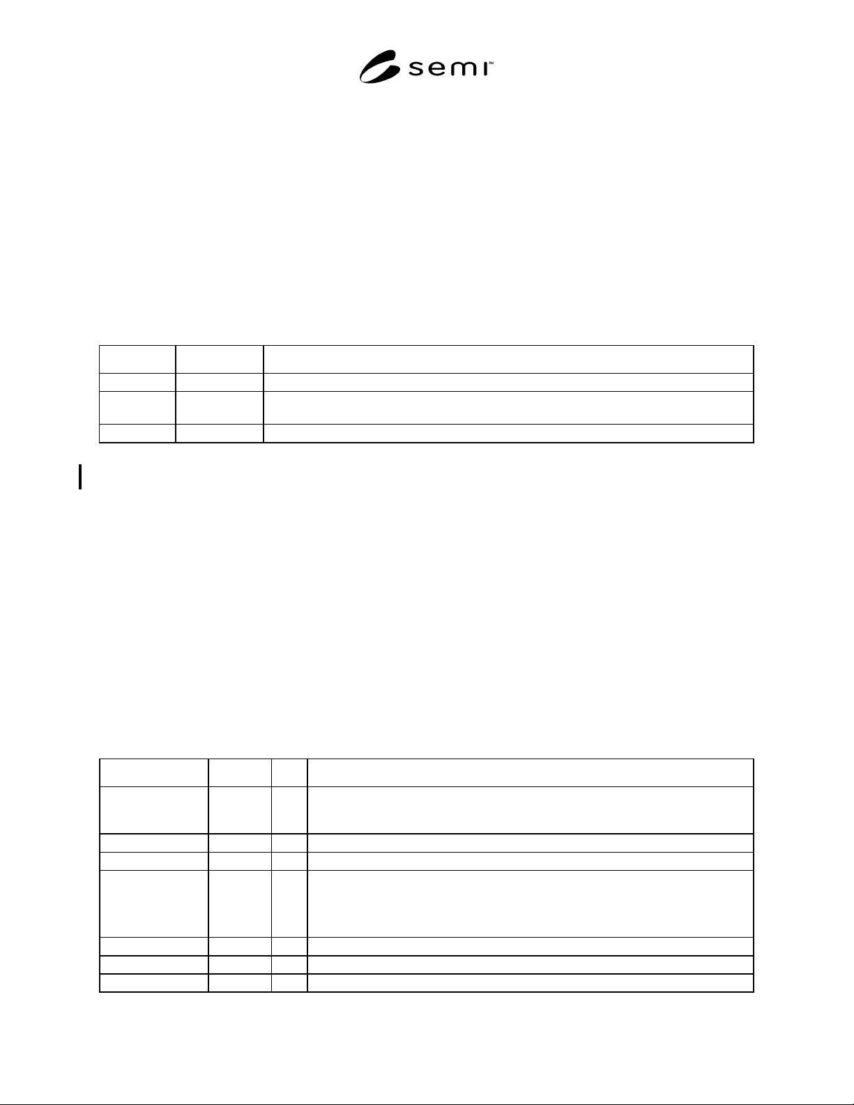
7.1 The substrate map data item specifications defined in this document are shown in Table 2. The columns in this
table are described in the following sections.
7.1.1 Item Name Column — the name by which the data item is referenced.
7.1.2 Data Type Column — the type of the data as defined in Table 1.
Table 1 Data Types and Sizes
Type Size Definition
String 0–32767 A string of ASCII characters from zero to “Size” characters in length.
Integer 1,2,4 An integer value that may be represented by “Size” bytes. E.g., if Size = 2 then the value may
be –32768 to 32767.
Float 4 IEEE single-precision 32-bit floating point type [IEEE 754-1985]
7.1.2.1 Generic data type definitions are used so that the data item definitions may be shared by several other
standards, which may have their own distinct data type representations.
7.1.3 Size Column — the maximum number of characters that may be used to represent the data.
7.1.4 Description Column — describes what the data item is and what value restrictions it has.
7.2 Coordinate System Conventions
7.2.1 Whenever reference is made to rows, columns, X or Y they are defined as follows.
7.2.2 The X axis is the horizontal axis from left to right when the substrate is rotated according to [Orientation] in
Table 2. Columns increase along the X axis. Column zero is the column just before the left (or right, depending on
OriginLocation) column containing measured devices.
7.2.3 The Y axis is the vertical axis from bottom to top when the substrate is rotated according to [Orientation] in
Table 2. Rows increase along the Y axis. Row zero is the row just before the extreme top (or bottom depending on
OriginLocation) row containing measured devices.
7.2.4 Columns increase along the X-axis. Rows increase along the Y-axis.
Table 2 Substrate Map Data Items
Item Name Data Type Size Description
FormatRevision String 256 Specifies the exact name and revision of the format used to represent substrate map
data. This field can be used by a parser to automatically determine the format of the
remaining substrate map data.
ProductId String 256 Product identifier
LotId String 32 Production lot identifier for this data.
Orientation Integer 2 The orientation of the substrate in relation to the map data.
This variable will increase in the right (clockwise) direction from 0° .
This item may be used to specify that the map data be rotated. Since the map data is
rectangular, only the values 0, 90, 180, and 270 are allowed in that case.
WaferSize Integer 2 Diameter of Wafer in millimeters.
DeviceSizeX Float 4 Device size on X axis in microns
DeviceSizeY Float 4 Device size on Y axis in microns