semi合集-English.pdf - 第7348页
SEMI MF1390-0704 © SEMI 2004 8 Table R1-2 Examples of Gravit y Effect Errors NOTICE: SEMI makes no warranties or repr esentations as to the suitability of the standard s set forth herein for any particular application. T…
SEMI MF1390-1104 © SEMI 2004 7
RELATED INFORMATION 1
MEASUREMENT ERRORS DUE TO DIFFERENCES IN DIAMETER AND
THICKNESS BETWEEN A REPRESENTATIVE WAFER AND A WAFER
UNDER TEST
NOTICE: This related information is not an official part of SEMI MF1390. This related information was approved
for publication by full letter ballot on April 22, 2004.
R1-1 The sag, or deflection induced by gravity at the
edge of a wafer supported at its center, in m, has been
estimated
3
as:
2
4
2
48
32
)103(
t
KD
Et
kgdD
S
(R1-1)
where:
S =
deflection , in m,
k = geometrical constant (=0.5854),
g = gravitational constant (980 cm/s
2
),
d = density of silicon (2.329 g/cm
3
),
E =
Young’s modulus (~1.610
12
dyne/cm
2
,
D = nominal wafer diameter, in mm, and
t =
nominal wafer thickness, in m.
K, the constant of proportionality is therefore equal to
7.83 10
3
m
3
/mm
4
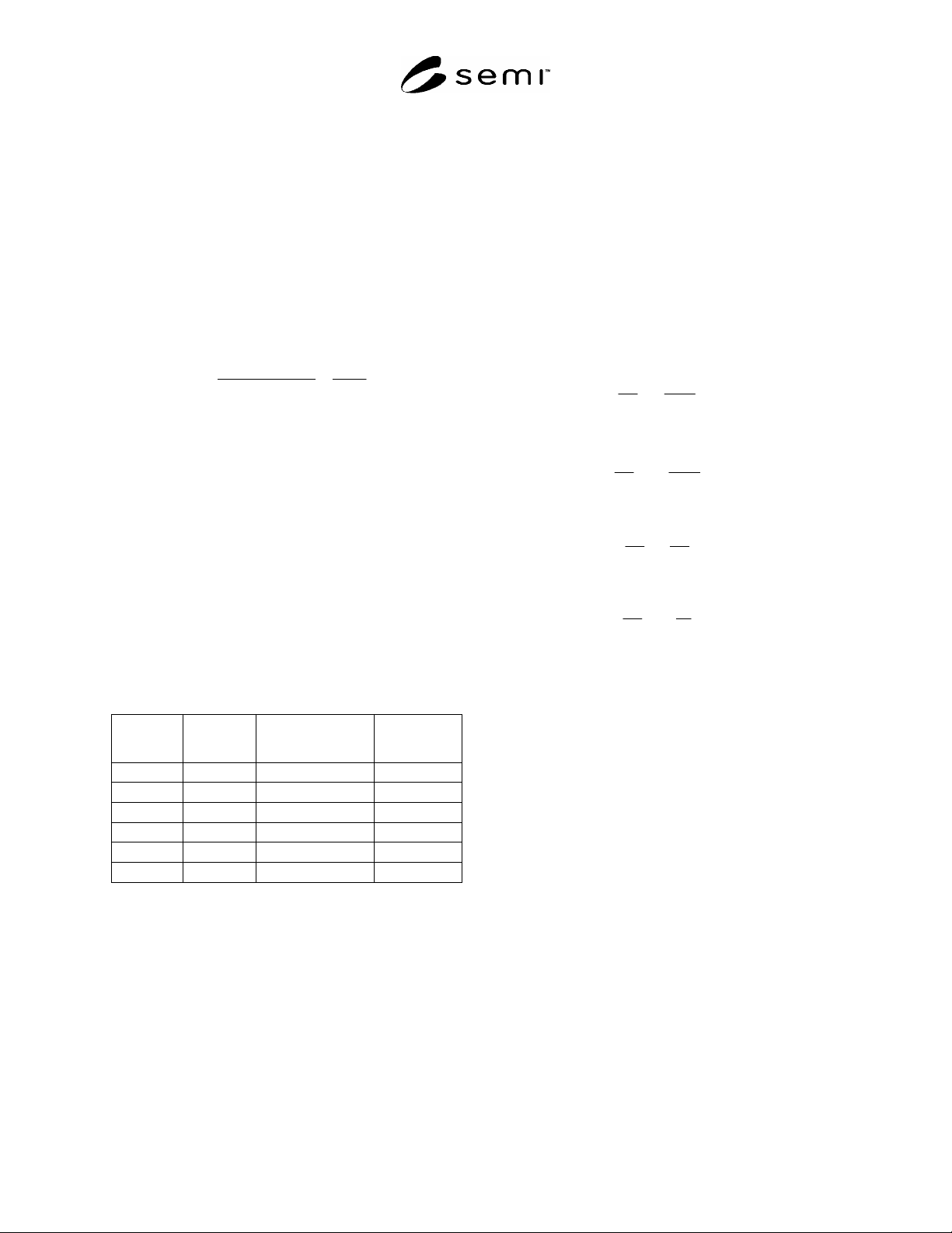
. Table R1-1 gives estimated
values of sag in micrometers for 100 mm through 300
mm diameter wafers with thickness and diameter as
specified in SEMI M1.
Table R1-1. Estimated Sag, in
m, of Wafers of
Nominal Diameter and Thickness
Diameter,
mm
Thickness,
m
SEMI M1 Reference Estimated Sag,
m
300 775 SEMI M1.15 105.6
200 725 SEMI M1.9 23.8
150 675 SEMI M1.8 8.7
150 625 SEMI M1.13 10.1
125 625 SEMI M1.7 4.9
100 525 SEMI M1.5 2.8
R1-2 For small variations about the nominal values of
diameter and thickness, the relative change of the
gravity effect is 4 times the relative change of the
diameter and 2 times the relative change of thickness:
2
3
4
t
Kd
d
S
(R1-2)
and
3
4
2
t
Kd
t
S
(R1-3)
Therefore the relative changes are as follows:
d
d
S
S
4 (R1-4)
and
t
t
S
S
2 (R1-5)
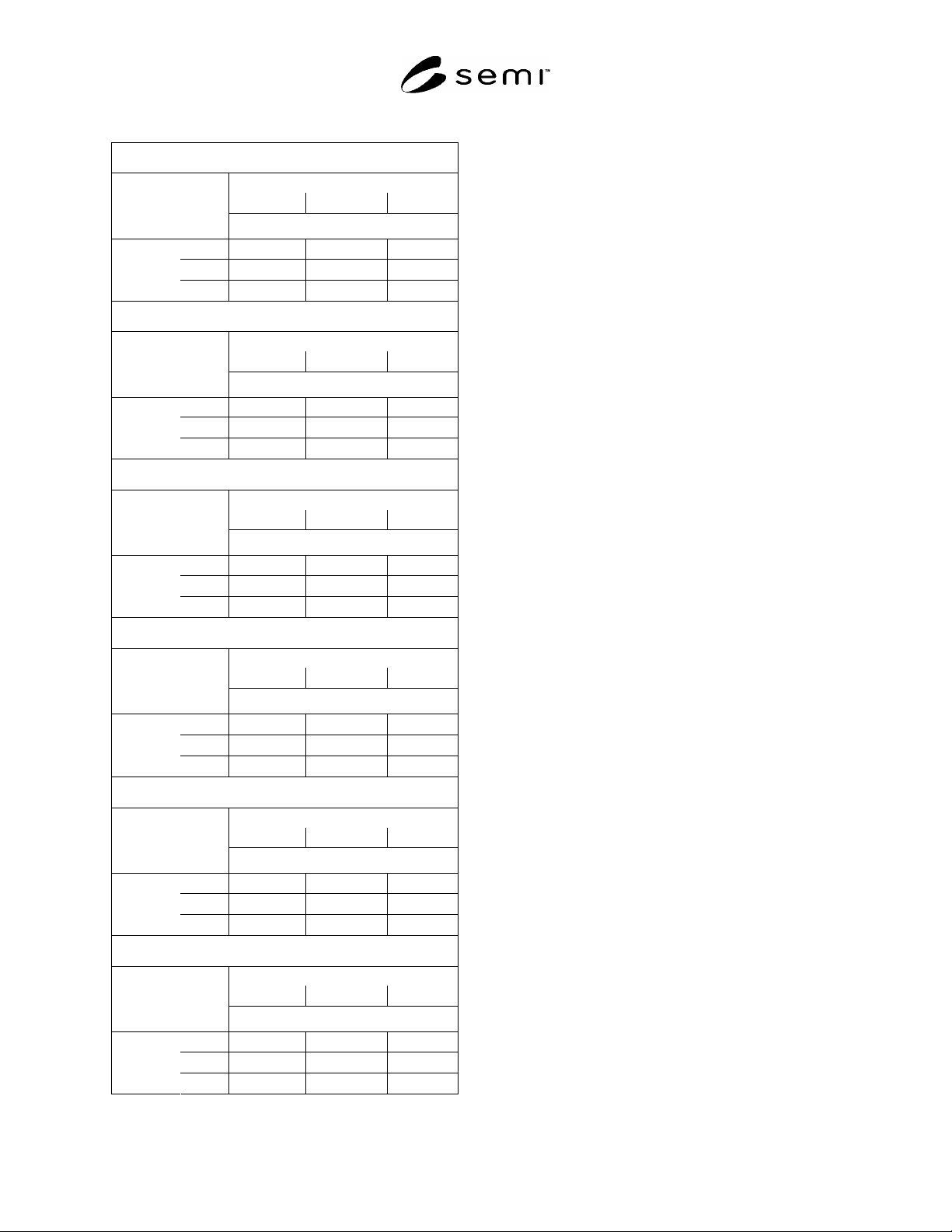
R1-3 Table R1-2 gives examples of worst-case gravity
effect errors (in micrometers), for 100 mm through 300
mm diameter wafers with thickness and diameter toler-
ances as specified in SEMI M1.
SEMI MF1390-0704 © SEMI 2004 8
Table R1-2 Examples of Gravity Effect Errors
NOTICE: SEMI makes no warranties or representations
as to the suitability of the standards set forth herein for any
particular application. The determination of the suitability
of the standard is solely the responsibility of the user.
Users are cautioned to refer to manufacturer's instructions,
product labels, product data sheets, and other relevant
literature, respecting any materials or equipment
mentioned herein. These standards are subject to change
without notice.
By publication of this standard, Semiconductor Equipment
and Materials International (SEMI) takes no position
respecting the validity of any patent rights or copyrights
asserted in connection with any items mentioned in this
standard. Users of this standard are expressly advised that
determination of any such patent rights or copyrights, and
the risk of infringement of such rights are entirely their
own responsibility.
300 mm Diameter Wafers
Actual Diameter, mm
299.8 300.0 300.2
Gravity Effect Errors,
m
755 3.90 5.67 5.96
775
1.68
0.00 0.28
Actual
Thickness,
m
795
6.84 5.25 4.98
200 mm Diameter Wafers
Actual Diameter, mm
199.8 300.0 200.2
Gravity Effect Errors,
m
705 0.77 1.37 1.47
725
0.57
0.00 0.10
Actual
Thickness,
m
745
0.52 1.26 1.17
150 mm Diameter Wafers
Actual Diameter, mm
149.8 150.0 150.2
Gravity Effect Errors,
m
655 0.49 0.54 0.59
675
0.05
0.00 0.05
Actual
Thickness,
m
695
0.54 0.49 0.45
150 mm Diameter Wafers
Actual Diameter, mm
149.8 150.0 150.2
Gravity Effect Errors,
m
610
0.45
0.51 0.56
625
0.05
0.00 0.05
Actual
Thickness,
m
640
0.52 0.47 0.42
125 mm Diameter Wafers
Actual Diameter, mm
124.5 125.0 125.5
Gravity Effect Errors,
m
605 0.25 0.33 0.41
625
0.08
0.00 0.08
Actual
Thickness,
m
645
0.37 0.30 0.22
100 mm Diameter Wafers
Actual Diameter, mm
99.5 100.0 100.5
Gravity Effect Errors,
m
505 0.17 0.23 0.29
525
0.06
0.00 0.06
Actual
Thickness,
m
545
0.26 0.20 0.15
Copyright by SEMI® (Semiconductor Equipment and Materials
International), 3081 Zanker Road, San Jose, CA 95134. Reproduction of
the contents in whole or in part is forbidden without express written
consent of SEMI.

SEMI MF1391-0704 © 2004 1
SEMI MF1391-0704
TEST METHOD FOR SUBSTITUTIONAL ATOMIC CARBON CONTENT
OF SILICON BY INFRARED ABSORPTION
This test method was technically approved by the Global Silicon Wafer Committee and is the direct
responsibility of the North American Silicon Wafer Committee. Current edition approved for publication by
the North American Regional Standards Committee on March 14, 2004. Initially available at
www.semi.org
May 2004; to be published July 2004. Original edition published by ASTM International as ASTM F 1389-
92. Last previous edition SEMI MF1389-00.
1 Purpose
1.1 Carbon may have an important role in defect
formation processes. Some laboratories have attributed
carbon as being involved in the formation of swirl.
Carbon has also been shown to serve as a nucleation
center for the precipitation of oxygen.
1.2 Although electrically inactive, substitutional carbon
causes stress that can be observed by X-ray topography.
1.3 Direct effects on the reverse bias characteristics of
power devices and annealing problems in neutron
transmutation doped silicon have been associated with
carbon.
1.4 This test method has applicability in production
control, materials research, quality assurance, and
materials acceptance.
2 Scope
2.1 This referee test method
1
covers the determination
of substitutional carbon concentration in single crystal
silicon. Because carbon may also reside in interstitial
lattice positions when in concentrations near the solid
solubility limit, the results of this test method may not
be a measure of the total carbon concentration at such
concentrations.
2.2 The useful range of carbon concentration
measurable by this test method is from the maximum
amount of substitutional carbon soluble in silicon down
to about 0.1 parts per million atomic (ppma), that is,
5 × 10
15
cm
−3
for measurements at room temperature,
1 This test method was developed in cooperation with the Silicon
Technologies Committee of the Japan Electronics and Information
Technology Industries Association (JEITA). It is essentially
equivalent to JEITA EM-9503, Standard Test Method for
Substitutional Atomic Carbon Content of Silicon by Infrared
Absorption, which is available from JEITA, 3rd floor, Mitsui
Sumitomo Kaijo Bldg. Annex, 11, Kanda-Surugadai 3-chome,
Chiyoda-ku, Tokyo 101-0062, Japan, Web site:
www.jeita.or.jp
. DIN
50438/2, Testing of Inorganic Semiconductor Materials:
Determination of the Impurity Content in Silicon by Means of
Infrared Absorption; Carbon, is also a method for measuring the
substitutional carbon content of silicon. It differs in some aspects,
including different conversion coefficients, from this test method. It
is available from Beuth Verlag GmbH, Burggrafenstrasse 4-10, D-
1000 Berlin 30, Germany.
and down to about 0.01 ppma, that is, 0.5 × 10
15
cm
−3
at cryogenic temperatures (below 80 K).
2.3 This test method utilizes the relationship between
carbon concentration and the absorption coefficient of
the infrared absorption band associated with
substitutional carbon in silicon. At room temperatures
(about 300 K), the absorption band peak is at 605 cm
−1
or 16.53 µm. At cryogenic temperatures (below 80 K),
the absorption band peak is at 607.5 cm
−1
or 16.46 µm.
2.4 This test method is applicable to slices of silicon
with resistivity higher than 3 Ω·cm for p-type and
higher than 1 Ω·cm for n-type. Slices can be any
crystallographic orientation and should be polished on
both surfaces.
2.5 This test method is intended to be used with
infrared spectrophotometers that are equipped to
operate in the region from 2000 to 500 cm
−1
(5 to 20
µm).
2.6 This test method provides procedure and calculation
sections for the cases where thickness values of test and
reference specimens are both closely and not closely
matched.
NOTICE: This standard does not purport to address
safety issues, if any, associated with its use. It is the
responsibility of the user of this standard to establish
appropriate safety and health guides and determine the
applicability of regulatory or other limitations prior to
use.
3 Limitations
3.1 Stray light that reaches the detector tends to reduce
the calculated absorbance value and thereby reduces the
reported carbon concentration.
3.2 The carbon level of the reference slice should be
less than 2 × 10
15
atoms/cm
3
(0.04 ppma) to minimize
the comparative error at room temperature. The
detection limit at cryogenic temperatures (below 80 K)
is about 0.01 ppma. Obtaining reference samples much
below 0.01 ppma in carbon content may prove to be
difficult. Therefore the measurement of very low
carbon content silicon near the 0.01 ppma detection
limit is necessarily a comparative measurement only.