semi合集-English.pdf - 第5201页
SEMI M37-0699 © SE MI 1999 2 Figure 1 Countin g position s for a 50 mm diameter wafer NOTICE: These st andards do not purport to addres s safety issues, if any, ass o ciated with their use. It is the responsibility of t …

SEMI M37-0699 © SEMI 19991
SEMI M37-0699
TEST METHOD FOR MEASURING ETCH PIT DENSITY (EPD) IN LOW
DISLOCATION DENSITY INDIUM PHOSPHIDE WAFERS
This test method was technically approved by the Global Compound Semiconductor Committee and is the
direct responsibility of the Japanese Compound Semiconductor Materials Committee. Current edition
approved by the Japanese Regional Standards Committee on March 17, 1999. Initially available at
www.semi.org April 1999; to be published June 1999.
1 Purpose
1.1 This document provides a method to measure etch
pit density (EPD) in low dislocation density InP wafers.
2 Scope
2.1 This test method describes a procedure to measure
EPD of 50 mm diameter round InP wafers with an EPD
of less than 5000/cm
2
.
2.2 This standard does not purport to address all of the
safety issues. It is the responsibility of the user of this
standard to establish appropriate safety and health
practices and to determine the applicability of
regulations prior to use of the test method.
3 Referenced Document
3.1 ASTM Standard
F 140-92 — Test Method for Crystallographic
Perfection of Gallium Arsenide by Molten Potassium
Hydroxide (KOH) Etch Technique.
4 Apparatus
4.1 Microscope — Measuring field should be 1 mm
2
or larger.
NOTE: For accurate EPD measurement, accurate area of the
measuring field should be measured by a standard scale.
5 Procedure
5.1 Orient the ingot so that the front surface normal
direction of the sample is parallel to the <100> within
5°, and then cut a wafer from the ingot.
5.2 Polish the wafer to form a mirror finish.
Afterwards, the wafer must be cleaned and dried.
5.3 Mix phosphoric acid (H
3
PO
4
) and hydrobromic
acid (HBr) in a beaker. The ratio of each acid is H
3
PO
4
:
HBr=2:1.
5.4 Immerse the wafer in the mixed acid for 3 minutes
at room temperature.
5.5 Rinse the wafer with deionized water and then dry.
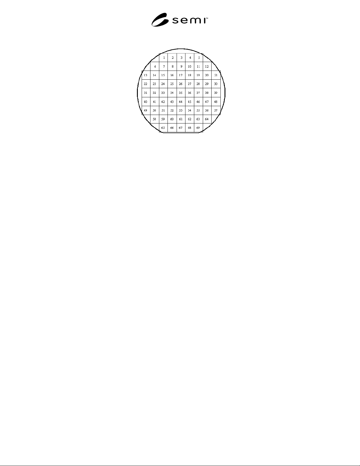
5.6 The counting positions are shown in Figure 1. The
counting points are located in the center of each mesh.
The mesh size is 5 mm and the total number of
counting positions is 69. Position 35 is located at the
center of the wafer.
5.7 Count and record the number of etch pits for
which the cores are in the measuring field. If the pits
are crowded and are difficult to count, increase the
magnification. After that count the etch pits and record
the results as well as the microscope magnification.
5.8 Repeat Section 5.8 for all other positions, 2
through 69.
6 Calculations
6.1 The EPD in each measuring field is the number of
pits counted divided by the area.
EPD = (Number of pits) / Area
For example, if the size of measuring field is exactly 1
mm × 1 mm, the area is 0.01 cm
2
.
7 Report
7.1 There are several forms that are possible for
reporting the EPD, for example the average EPD of all
the positions or the area less than some specified value
or map of EPD for the entire wafer, etc. An appropriate
report form should be decided between the supplier and
the user.
SEMI M37-0699 © SEMI 1999 2
Figure 1
Counting positions for a 50 mm diameter wafer
NOTICE: These standards do not purport to address
safety issues, if any, associated with their use. It is the
responsibility of the user of these standards to establish
appropriate safety and health practices and determine
the applicability of regulatory limitations prior to use.
SEMI makes no warranties or representations as to the
suitability of the standards set forth herein for any
particular application. The determination of the
suitability of the standard is solely the responsibility of
the user. Users are cautioned to refer to manufacturer's
instructions, product labels, product data sheets, and
other relevant literature respecting any materials
mentioned herein. These standards are subject to
change without notice.
The user's attention is called to the possibility that
compliance with this standard may require use of
copyrighted material or of an invention covered by
patent rights. By publication of this standard, SEMI
takes no position respecting the validity of any patent
rights or copyrights asserted in connection with any
item mentioned in this standard. Users of this standard
are expressly advised that determination of any such
patent rights or copyrights, and the risk of infringement
of such rights are entirely their own responsibility.
Copyright by SEMI® (Semiconductor Equipment and Materials
International), 3081 Zanker Road, San Jose, CA 95134. Reproduction o
f
the contents in whole or in part is forbidden without express written
consent of SEMI.

SEMI M38-1104 © SEMI 1999, 2004 1
SEMI M38-1104
SPECIFICATION FOR POLISHED RECLAIMED SILICON WAFERS
This specification was technically approved by the Global Silicon Wafer Committee and is the direct
responsibility of the North American Silicon Wafer Committee. Current edition approved by the North
American Regional Standards Committee on August 16, 2004. Initially available at www.semi.org
September 2004; to be published November 2004. Originally published September 1999; previously
published November 2001.
NOTICE: This document was completely rewritten in
2004.
1 Purpose
1.1 Silicon wafers are often subjected to reclaim
processes in order to improve manufacturing efficiency
in device production. A reclaimed wafer is one that has
been re-conditioned for subsequent utilization.
1.2 This specification covers requirements for
reclaimed silicon wafers to be used for testing and
process monitoring in semiconductor manufacturing.
1.3 In some instances for 300 mm wafers with supplier
marked back surfaces, it is necessary to re-inscribe the
mark after one or more reclaim cycles. Consequently,
this specification also includes an appendix that covers
the re-inscription of such wafers.
NOTE 1: Issues related to the re-inscription of such 300 mm
wafers are discussed in Related Information 1.
2 Scope
2.1 This specification divides reclaimed wafers into
four application categories: Mechanical, Furnace,
Particle, and Lithography and provides tables of the
specification requirements for each category. Thus, a
prospective purchaser of reclaimed silicon wafers needs
to know which application matches his or her
requirements.
2.2 Only requirements for some attributes are specified
in Tables 1 and 2. Other requirements are indicated to
be “customer specified” which means that the customer
may specify a requirement for that particular attribute,
“as-supplied” which means that the attribute has
whatever value was supplied in the wafer delivered (or
used) for reclaim, and “unspecified” which means that
the attribute is not specified and for which the wafer
does not need to be tested.
2.3 In addition to the general categories listed in
Section 2.1, this specification provides requirements for
reclaimed wafers intended for use in advanced device
production, including devices in the 180 and 130 nm
technology generations in a third table.
2.4 This specification is directed specifically to silicon
wafers with one or both polished surfaces. If the wafers
have epitaxial deposits, the attributes of the epitaxial
layer are not included the specification requirements.
2.5 This specification covers reclaim wafers that are
either customer-supplied or third party-sourced. The
user should exercise caution when sourcing materials
with unknown thermal histories, unknown bulk
contamination, or unknown deposits, such as gold (Au)
films.
2.6 For applications placing higher demands on silicon
wafers such as particle counting, measuring pattern
resolution in a photolithography process, or surface ion
contamination monitoring, the customer may want to
reference SEMI M1, SEMI M8, or SEMI M24.
2.7 For referee purposes, U.S. customary units shall be
used for wafers of 2- and 3-inch nominal diameter and
SI (System International), commonly called metric,
units for 100 mm and larger diameter wafers.
NOTICE: This standard does not purport to address
safety issues, if any, associated with its use. It is the
responsibility of the users of this standard to establish
appropriate safety and health practices and determine
the applicability of regulatory or other limitations prior
to use.
3 Referenced Standards
3.1 SEMI Standards
SEMI M1 — Specifications for Polished
Monocrystalline Silicon Wafers
SEMI M8 — Specification for Polished
Monocrystalline Silicon Test Wafers
SEMI M18 — Format for Silicon Wafer Specification
Form for Order Entry
SEMI M24 — Specification for Polished
Monocrystalline Silicon Premium Wafers
SEMI M31 — Provisional Mechanical Specification for
Front Opening Shipping Box Used to Transport and
Ship 300 mm Wafers
SEMI M45 — Provisional Shipping System for 300
mm Wafer Shipping System
SEMI MF1241 — Terminology of Silicon Technology