semi合集-English.pdf - 第7606页
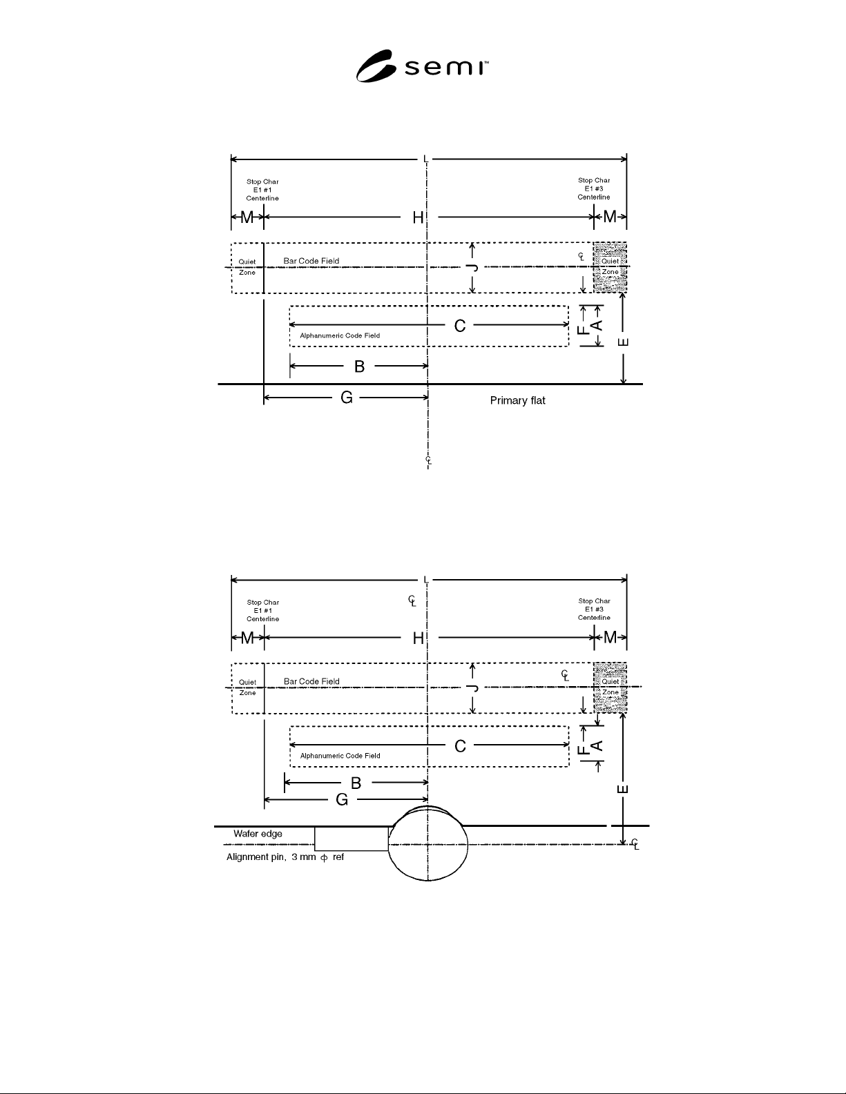
SEMI T1-95 © SEMI 1993, 2003 7 Figure 3 Code Field Locations for Flatted Wafers Figure 4 Code Field Locations for Notched Wafers
SEMI T1-95 © SEMI 1993, 2003 6
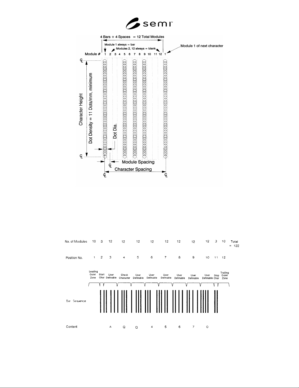
Figure 1
BC-412 Data Character Construction
NOTE 4: Each bar code character contains four bars and four spaces. A space is one or more contiguous blanks. Module 1 is
always a bar; the other three bars are distributed among modules 3−11; modules 2 and 12 are always spaces. One or more blanks
which comprise a space must occur between bars.
Figure 2
BC-412 Character Position and Module Content
SEMI T1-95 © SEMI 1993, 2003 7
Figure 3
Code Field Locations for Flatted Wafers
Figure 4
Code Field Locations for Notched Wafers

SEMI T1-95 © SEMI 1993, 2003 8
NOTICE: SEMI makes no warranties or representations as to the suitability of the standards set forth herein for any
particular application. The determination of the suitability of the standard is solely the responsibility of the user.
Users are cautioned to refer to manufacturer's instructions, product labels, product data sheets, and other relevant
literature, respecting any materials or equipment mentioned herein. These standards are subject to change without
notice.
By publication of this standard, Semiconductor Equipment and Materials International (SEMI) takes no position
respecting the validity of any patent rights or copyrights asserted in connection with any items mentioned in this
standard. Users of this standard are expressly advised that determination of any such patent rights or copyrights, and
the risk of infringement of such rights are entirely their own responsibility.