semi合集-English.pdf - 第5838页
SEMI P31-0304 © SEMI 1997, 2004 1 SEMI P31-0304 PRACTICE FOR CATALOG PU BLICATION FOR CHEMICAL AMPLIFIED (CA) PHOT ORESIST PARAMETER This practice was technically approved by the Gl obal Micropatterning Committ ee and is…

5 SEMI P30-0997 © SEMI 1997, 2004
6.27 Standard Layout Diagram — List the standard
layout when installing equipment. Equipment
installation conditions can be listed in the diagram.
6.28 Mass — List in kg.
6.29 Permissible Floor Weight — List in kg/m
2
.
6.30 Permissible Stray Magnetic Field — List in T,
and list effective values or peak values separately.
6.31 Permissible Floor Vibration — List the maximum
vibration level in dB in the 1–80 Hz frequency range.
The vibration acceleration level La is found from the
following equation:
La = 20l og ( a / a
o
)
Here,
a — Is the effective value of the vibration acceleration
when the sensory vibration is not corrected:
a
o
— (Standard vibration acceleration) (10
-6
m / s
2
)
6.32 Permissible Air Vibration — List the maximum
sound level in dB in the 20 Hz – 8 kHz frequency
range. The sound pressure level La is found from the
following equation:
La = 20l og (a / a
o
)
Here, a is the effective value for sound pressure in Pa
units.
a
o
(Standard sound pressure) (20 Pa)
6.33 Reference Specification — List guideline as the
reference specification.
NOTICE: SEMI makes no warranties or
representations as to the suitability of the standard set
forth herein for any particular application. The
determination of the suitability of the standard is solely
the responsibility of the user. Users are cautioned to
refer to manufacturer’s instructions, product labels,
product data sheets, and other relevant literature
respecting any materials or equipment mentioned
herein. These standards are subject to change without
notice.
By publication of this standard, SEMI takes no position
respecting the validity of any patent rights or copyrights
asserted in connection with any item mentioned in this
standard. Users of this standard are expressly advised
that determination of any such patent rights or
copyrights, and the risk of infringement of such rights,
are entirely their own responsibility.
Copyright by SEMI® (Semiconductor Equipment and Materials
International), 3081 Zanker Road, San Jose, CA 95134. Reproduction of
the contents in whole or in part is forbidden without express written
consent of SEMI.

SEMI P31-0304 © SEMI 1997, 2004 1
SEMI P31-0304
PRACTICE FOR CATALOG PUBLICATION FOR CHEMICAL
AMPLIFIED (CA) PHOTORESIST PARAMETER
This practice was technically approved by the Global Micropatterning Committee and is the direct
responsibility of the Japanese Micropatterning Committee. Current edition approved by the Japanese
Regional Standards Committee on January 9, 2004. Initially available at www.semi.org February 2004; to be
published March 2004. Originally published September 1997.
1 Purpose
1.1 The purpose of this document is to provide a
baseline for publication of chemical amplified (CA)
photoresist parameters.
2 Scope
2.1 This document applies to CA photoresist used for
semiconductor manufacturing.
2.2 This document is used as the guide to evaluate
photoresist process parameters.
2.3 This document is not applicable for quality
assurance.
NOTICE: This standard does not purport to address
safety issues, if any, associated with its use. It is the
responsibility of the users of this standard to establish
appropriate safety and health practices and determine
the applicability of regulatory or other limitations prior
to use.
3 Referenced Standards
None.
4 Terminology
4.1 Abbreviations and Acronyms
4.1.1 PEB — post exposure bake
5 Description
NOTE 1: The following parameters for CA photoresist
publication and test conditions should be described in the
catalog.
5.1 Resist, overcoat and developer commercial name
5.2 Temperature and humidity
5.3 Environmental conditions (see Section 6)
5.4 Ammonia concentration measurement method (see
Section 7)
5.5 Delay time dependency (see Section 8)
5.6 PEB temperature dependency (see Section 9)
5.7 PEB time dependency (see Section 10)
5.8 Substrate dependency (see Section 11)
5.9 Measurement Conditions
5.9.1 Resist Coating and Development
5.9.1.1 Resist baking method (contact baking or
proximity baking)
5.9.1.2 Resist pre-baking temperature and time
5.9.1.3 Resist PEB temperature and time
5.9.1.4 Development time
5.9.1.5 Resist thickness
5.9.2 Exposure
5.9.2.1 Illumination conditions (NA, σ, etc. )
5.10 Equipment Name
5.10.1 Exposure equipment
5.10.2 SEM equipment
5.10.3 Ammonia concentration measurement equip-
ment
6 Environmental Conditions
6.1 Ammonia Concentration — It is recommended to
measure all CA photoresist parameters under the
condition that the ammonia concentration is less than
10 µg/m
3
.
NOTE 2: CA photoresist is sensitive to the atmosphere,
especially to ammonia. Acid from photoacid generator upon
exposure is neutralized by the basic material in atmosphere
like ammonia.
7 Ammonia Concentration Measurement
Method
7.1 The ammonia concentration is measured by ion
chromatography or another method which is capable to
determine the ammonia concentration quantitatively
less than 10 µg/m
3
. The measurement equipment is
calibrated with a standard ammonia solution.
SEMI P31-0304 © SEMI 1997, 2004 2
8 Delay Time Dependency
NOTE 3: This section defines process conditions and procedures to obtain the delay time dependency.
8.1 Resist Coating and Pre-baking — Resist should be coated on a substrate. Suppliers should be notified of the
kind of substrate and underlying film. After pre-baking, the resist thickness should be chosen the bottom of swing
curve between 0.3–0.5 µm. Thickness could be changed in accordance with exposure wavelength. The actual
thickness should be notified.
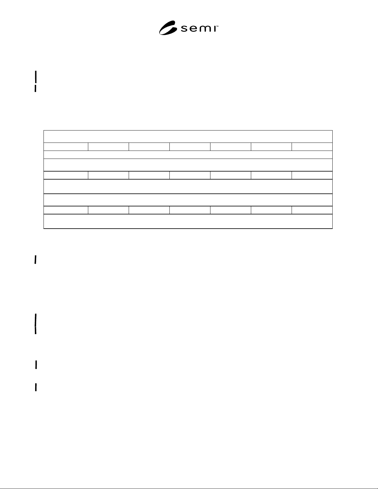
8.2 Delay Time — Delay time between resist coating and exposure, exposure and PEB, and PEB and development
used for obtaining delay time dependency parameters are defined in Table 1.
Table 1 Delay Time Condition
Resist coating to exposure delay time
0 min. 1 hour 6 hour 24 hour
NOTE: Normal sequential procedure without intentional delay between exposure and PEB as well as PEB and development.
Exposure to PEB delay time
0 min. 10 min. 30 min. 1 hour 2 hour 24 hour
NOTE: Normal sequential procedure without intentional delay between resist coating and exposure as well as PEB and
development.
PEB to development delay time
0 min. 10 min. 30 min. 1 hour 24 hour
NOTE: Normal sequential procedure without intentional delay between resist coating and exposure time as well as exposure and
PEB.
NOTE: Zero minutes (0 min.) is defined as normal sequential procedure without intentional delay.
8.3 Measurement
8.3.1 After each time delay, fabricated 0.10 µm and 0.15 µm line and space patterns should be measured by SEM.
8.3.2 Record the measured pattern size.
8.3.3 Make the plotting of pattern size vs. delay time.
9 PEB Temperature Dependency
NOTE 4: This section defines process conditions and procedures to obtain the PEB temperature dependency.
9.1 Resist Coating and Pre-baking — Resist should be coated on a substrate. Suppliers should be notified of the
kind of substrate and underlying film. After pre-baking, the resist thickness should be chose the bottom of the swing
curve between 0.3–0.5 µm. Thickness could be changed in accordance with exposure wavelength. The actual
thickness should be notified.
9.2 Measurement
9.2.1 Ten points of temperature should be selected within ± 20 °C from the optimized PEB temperature.
9.2.2 Record the measured pattern size.
9.2.3 Make the plotting of pattern width vs. PEB temperature. At least 6 to 8 points of pattern width should be
plotted within the deviation of ± 10% from the optimized line width of 0.10 µm and 0.15 µm line and space patterns.
9.2.4 The cross section of resist patterns is observed and compared each other with standard sample. One should be
selected from the optimized condition and the other one should be selected from the sample deviated around 10%
from standard one.