semi合集-English.pdf - 第7475页
SEMI MF1618-1104 © SEMI 2004 5 9.3.2 Standard Devi ation Uniformity, SUP , in percent: 100 (%) x s SUP (4) 10 Report 10.1 Repo rt the fol lowing informat ion when describin g the uniformity of a specific thin film pa…

SEMI MF1618-1104 © SEMI 2004 4
6 Summary of Practice
6.1 Measurements are made at the sites specified in the
chosen sampling plan using the appropriate
instrumentation and measurement procedure for the
film parameter of interest. Measures of the dispersion
of the values are obtained by simple statistics specified
for the sampling plans.
7 Apparatus
7.1 Four-probe Sheet Resistance, Eddy-current,
Mercury Probe CV, Spectroscopic Reflectometers,
Ellipsometers, Interferometers, and Stylus
Profilometers — Typical apparatus chosen according to
the type of material parameter being monitored. Others
may be chosen according to need. The instrumentation
should include such features as temperature monitoring
and control, EMI shielding, shielding from
illumination, etc. as is necessary for good practice of
that type of measurement. In addition, all
instrumentation must include the following:
7.1.1 Ability to center the wafer on the measurement
stage to an accuracy of 0.5 mm or better,
7.1.2 Vacuum chuck, or similar fixture, to secure the
wafer to the instrument stage during measurement,
7.1.3 Ability to locate the measurement points
specified in the chosen sampling plan to an accuracy of
0.5 mm or better, and
7.1.4 Ability to store all measurement data to perform
the required calculation of uniformity.
7.2 Capability of the instrumentation to perform one or
more of the following auxiliary data presentations is
highly recommended:
7.2.1 Generating a two-dimensional contour map of the
acquired data,
7.2.2 Generating a histogram of the raw data values,
and
7.2.3 Presenting the raw data as a time-series plot.
7.3 Capability to edit data and to blend or interpolate
data in conjunction with two-dimensional mapping may
be useful, but it should be done with caution.
8 Procedure
8.1 Calibrate the measurement system in accordance
with the manufacturer’s instructions or with the
applicable test method.
8.2 Place the wafer on the instrument stage so as to
locate the wafer center within 0.5 mm of the center of
the stage. For the purposes of this procedure, the wafer
center is considered to be defined by the intersection of
any two diameters that do not intersect a wafer flat or
orientation notch.
8.3 Select the sampling plan to be used from those
listed in Appendix 1 and proceed to take measurements
at all the specified locations. It may be necessary to
enter the coordinates of the desired sampling plan into
instrument software, or to work with the manufacturer
of the equipment to modify its software if the sampling
plans available in the instrument do not match the
requirements of Appendix 1.
8.4 Take measurements at all locations specified for
the selected sampling plan. Then quantify the
uniformity from the acquired data using the calculations
specified in Section 9.
9 Calculations
9.1
Calculate the mean,
x , and the standard deviation,
s, of the N measurement values, x
i
, as follows:
N
i
i
x
N
x
1
1
, and (1)
2/1
1
2
)(
1
1
N
i
i
xx
N
s (2)
9.2 Examine the data. If agreed upon between parties
to the test, reject values that are away from the mean by
more than three times the standard deviation calculated
in Section 9.1. Recalculate the mean and standard
deviation using Equations 1 and 2, where N is now the
reduced number of data points.
NOTE 1: It is generally advisable, through use of a time
series plot of the original data, or similar means, to inspect the
data just rejected for determination of measurement site
location and relation to adjacent measurement values.
NOTE 2: The calculation for standard deviation may be
made regardless of any systematic behavior of the underlying
distribution of measured values. However, when there is a
systematic spatial behavior to the measured values, the
standard deviation may not be used to estimate confidence
intervals or tolerance limits.
9.3 Calculate the following two statistics from the
complete data set or from the reduced data set if certain
measurements were rejected in Section 9.2. These two
statistics represent the range and the distribution of data
about the mean. The use of only one of these statistics
is at the discretion of the interested parties.
9.3.1 High-Low Variation, HLV, in percent:
200(%)
minmax
minmax
xx
xx
HLV
(3)

SEMI MF1618-1104 © SEMI 2004 5
9.3.2 Standard Deviation Uniformity, SUP, in percent:
100(%)
x
s
SUP (4)
10 Report
10.1 Report the following information when describing
the uniformity of a specific thin film parameter across
the surface of a wafer:
10.1.1
Wafer identification and diameter,
10.1.2 Operator and date,
10.1.3 Substrate type (orientation and doping, if
appropriate),
10.1.4 Generic film type, and reactor, run or process
information, as appropriate,
10.1.5
Film parameter measured and assumed material
constants used for analysis,
10.1.6 Sampling plan used,
10.1.7 Test method used by designation, if available, or
by brief description if no standard procedure is
available,
10.1.8
Test instrument manufacturer, model, options,
10.1.9 Total number of points measured; number of
points within 3-sigma; number of points used to
calculate HLV and SUP,
10.1.10 Calculated HLV(%), SUP(%), mean value (
x ),
and sample standard deviation, s.
10.2
Two-dimensional contour plot, data histogram, or
time series plot of measurement values may be included
if agreed upon between the parties to the test.
10.3 For a single-diameter sampling plan, also report
the angle between the diameter measured and the
fiducial axis.
11 Precision and Bias
11.1 Precision — The precision with which wafer
uniformity can be measured is governed by the
precision of the individual test method being used.
11.2
Bias — The bias associated with the wafer
uniformity measurements is also governed by the bias
of the individual test method being used.
11.3
The Precision and Bias sections of the test method
being used should be consulted.
NOTE 3: The Appendix
1
of SEMI MF81 gives, for the case
of sparse site sampling plans, an example of the propagation
of error from the basic measurement technique to the
determination of variation of material properties using that
technique.
11.4 The standard deviation and range calculations that
are specified in Section 9 are descriptive statistics or
figures of merit for describing the uniformity of the thin
film wafer in a simple and consistent manner, but they
are generally not appropriate for determining the
precision of the measurements.
12 Keywords
12.1 dielectric layers; epitaxial layers; ion implant;
metal films; sampling plans; semiconductor; silicon;
thin films; uniformity
1 This non-mandatory section will be called Related Information after
this standard has been reformatted and adopted through the SEMI
Standards process.
SEMI MF1618-1104 © SEMI 2004 6
APPENDIX 1
SAMPLING PLANS TO BE USED FOR WAFER UNIFORMITY
DETERMINATION
NOTICE: The material in this appendix is an official part of SEMI MF1618 and was approved by full letter ballot
procedures.
A1-1 Introduction
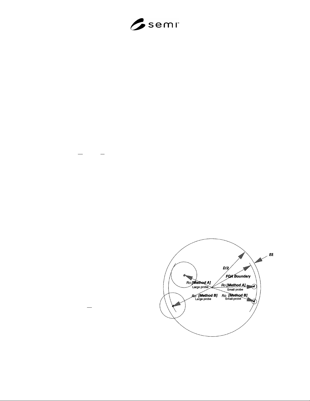
A1-1.1 For all plans, measurements are made within a
circular area defined by the radius, R
o
, between the
center of the wafer and the circle on which the centers
of the outermost measurement sites lie. Determine this
radius by either of the following methods:
A1-1.1.1
Method A — In this method, the outermost
edges of the measurement spots on the outermost radius
are tangent to the boundary of the fixed quality area
(FQA) as defined in SEMI M1:
)
2
(
2
d
EE
D
R
o
(A1-1)
where:
R
o
= radius of the outermost measurement circle (see
Figure A1-1),
D = nominal diameter of the wafer, for example,
100, 150, 200, or 300 mm,
EE = nominal wafer edge exclusion, which
determines the FQA, and
d = known or estimated diameter of the
measurement spot for the test instrument being
used (Note 1).
NOTE 1: The exact diameter of the measurement spot may
not be known for many types of measurements. Estimate the
diameter as 1.5 times the probe spacing for a four-point probe,
transducer radius for an eddy-current instrument, and apparent
beam spot radius for optical measurements if no other
information is available.
A1-1.1.2 Method B — In this method, the centers of the
measurement spots on the outermost radius are on the
boundary of the fixed quality area (FQA) as defined in
SEMI M1:
EE
D
R
o
2
(A1-2)
where the symbols are defined following Equation A1-
1.
A1-2 Selection of Method
A1-2.1 Neither of these methods is “better” than the
other; rather, there are tradeoffs.
A1-2.2
The location of every point in a multipoint
measurement pattern depends on the method chosen to
define the position of the outermost measurement sites.
Therefore, there may be differences between the two
methods for reported individual and statistical values.
A1-2.3
Data for a measurement site are usually reported
at the location corresponding with the center of the
measurement spot.
A1-2.4
Data from each measurement on the outermost
ring in Method A are not affected by the film properties
in the edge exclusion annulus outside the FQA.
However, in this case, data are not reported for
locations closer to the boundary of the FQA than the
measurement spot radius.
A1-2.5
Conversely, data from each measurement on the
outermost ring with Method B include contributions
from film properties both inside and outside the FQA.
In this case, measurement data is reported for locations
up to the boundary of the FQA, but establishing the
significance of including data influenced by film
properties outside the FQA is outside the scope of this
practice.
NOTE 2: Measurements obtained using a probe whose
effective measurement area extends beyond the edge of the
film inaccurately represent actual film properties.
Figure A1-1
FQA Boundary and Outermost Ring Radii, R
o
, for
Methods A and B