semi合集-English.pdf - 第5115页
SEMI M24-1103 © SEMI 1994, 2003 18 requested for monitor test wafer s. In act ual business, an additional specification of LL S, the size of which is around CD is us ed, however , the size is not standardized. TF propose…
SEMI M24-1103 © SEMI 1994, 2003 17
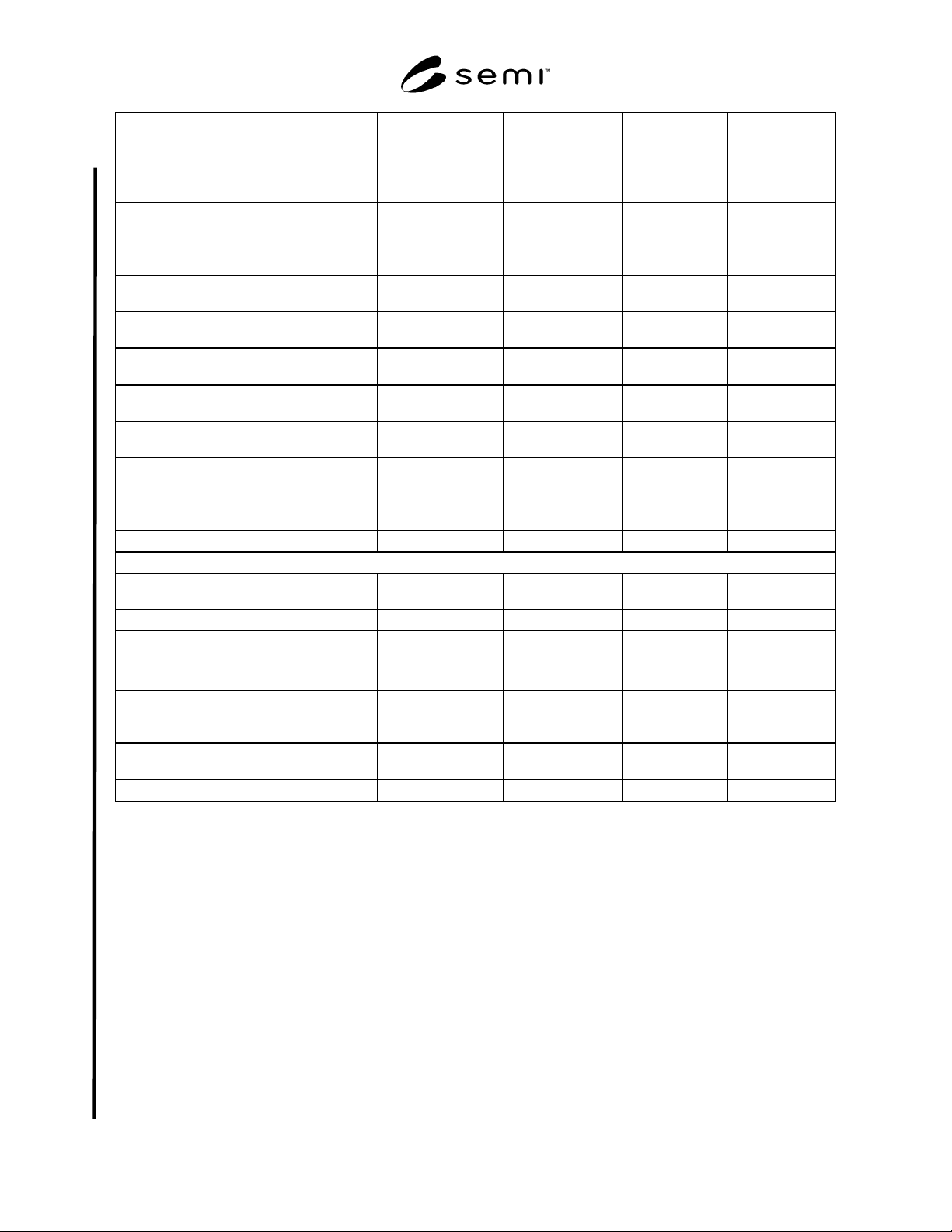
CLASSIFICATION ITEMS (SEMI M18) Particle Counting
Furnace & Thermal
Process
Lithography &
Patterning
Test Method
8.5 Contamination/Area None None None ASTM F 154, F
523, JIS H 614
8.6 Edge chips None None None ASTM F 154, F
523, JIS H 614
8.7 Cracks, Crow’s Feet None None None ASTM F 154, F
523, JIS H 614
8.8 Craters None None None ASTM F 154, F
523, JIS H 614
8.9 Dimples None None None ASTM F 154, F
523, JIS H 614
8.10 Grooves None None None ASTM F 154, F
523, JIS H 614
8.11 Mounds None None None ASTM F 154, F
523, JIS H 614
8.12 Orange Peel None None None ASTM F 154, F
523, JIS H 614
8.14 Saw Marks None None None ASTM F 154, F
523, JIS H 614
8.15 Dopant Striation Ring None None None ASTM F 154, F
523, JIS H 614
8.- Microroughness NS NS NS
9. BACK SURFACE VISUAL INSPECTION CHARACTERISTICS
9.1 Edge Chips None None None ASTM F 154, F
523, JIS H 614
9.6 Roughness, rms NS NS NS
9.7 Brightness (Gloss)
300 mm
200 mm
≥ 80%
User/Vendor
≥ 80%
User/Vendor
≥ 80%
User/Vendor
ASTM D 523,
JIS Z8741
9.8 Localized Light Scatterers (LLSs) NS NS NS ASTM F 523,
F 1620, F 1621,
JIS H 614
9.9 Scratches, Macro
≤ 0.25 × D mm ≤ 0.25 × D mm ≤ 0.25 × D mm
ASTM F 154, F
523, JIS H 614
9.10 Scratches, Micro NS NS NS ASTM F 154
NOTE 1: Nominal Edge Exclusion is proposed considering future trends referring ITRS Roadmap, however, more discussion will be necessary.
NOTE 2: ASTM F47-94 (Discontinued 1998) was replaced by ASTM Guide F1725, and ASTM F416-94 (Discontinued 1998) was replaced by
ASTM Practice F1727.
NOTE 3: Wafer ID Marking: For 300 mm wafers, Backsurface SEMI T7 mark in accordance with SEMI M1.15 is recommended. For 200mm
Wafers; Various types of ID (or No ID) are prevailed in the market.
NOTE 4: Flatness/Site SFQR(25 × 8mm □
) is proposed referring to the recent ITRS Roadmap discussion and also referring to discussion in Epi
SC for the specification guide for 90 nm node usage. Two types of scanning stepper are introduced in industry, with the site of 25 × 8 mm □ and
the site of 26 × 8 mm □.
NOTE 5: Surface metal measurement variation can be significant. Measured results are frequently larger that the actual value. Processes are
normally designed and controlled with median values to reduce the impact of measured variation.
NOTE 6: Visual techniques are neither sufficient nor appropriate for 90 nm design rules. Automatic surface inspection tools can be used for
reporting values such as scratches and haze. Test method and standardization for automatic surface inspection tools is under development, visual
inspection is now used as a supplemental method.
NOTE 7: LLSs (Localized Light Scatterers: 65 nm or 50 nm): Critical surface LLS size is proposed to be the half of CD, however, tools are not
well established. Some measurement tools have capability to measure 50 nm (nearly 1/2 of CD) LLS, however, some ones have not enough
capability, so that 50 nm count limit was transferred to 65nm count limit using draft international standard, ISO/DIS 14644-1 which follows the
equation: 65 nm LLS counts per wafer = 50 nm LLS counts per wafer/(65 nm /50 nm )
2
. These specification values shall be reviewed when the
evaluation techniques for distinguishing particle and COP are established and considering production capability.
NOTE 8: LLSs for Furnace & Thermal Process and Lithography & Patterning: New concept is proposed for LLSs for Furnace and Thermal
Process. The critical surface LLS size for prime wafer is proposed as a half size of CD in IRTS Roadmap. The half of CD is not necessarily

SEMI M24-1103 © SEMI 1994, 2003 18
requested for monitor test wafers. In actual business, an additional specification of LLS, the size of which is around CD is used, however, the size
is not standardized. TF proposes the additional LLS size as the same size as CD. This size is used for specifying LLS for Furnace & Thermal
Process Wafers.
NOTICE: SEMI makes no warranties or representations as to the suitability of the standards set forth herein for any
particular application. The determination of the suitability of the standard is solely the responsibility of the user.
Users are cautioned to refer to manufacturer's instructions, product labels, product data sheets, and other relevant
literature respecting any materials or equipment mentioned herein. These standards are subject to change without
notice.
The user's attention is called to the possibility that compliance with this standard may require use of copyrighted
material or of an invention covered by patent rights. By publication of this standard, SEMI takes no position
respecting the validity of any patent rights or copyrights asserted in connection with any item mentioned in this
standard. Users of this standard are expressly advised that determination of any such patent rights or copyrights, and
the risk of infringement of such rights, are entirely their own responsibility.
Copyright by SEMI® (Semiconductor Equipment and Materials
International), 3081 Zanker Road, San Jose, CA 95134. Reproduction o
f
the contents in whole or in part is forbidden without express written
consent of SEMI.

SEMI M25-95 © SEMI 1995, 2003 1
SEMI M25-95 (Withdrawn 1103)
SPECIFICATION FOR SILICON WAFERS FOR CALIBRATION OF
LIGHT POINT DEFECT WAFER INSPECTION SYSTEMS WITH
RESPECT TO THE DIAMETER OF POLYSTYRENE LATEX SPHERES
NOTICE: This document was balloted and approved
for withdrawal in 2003.
1 Purpose
1.1 This document describes the specifications to be
met by bare silicon wafers used for calibrating surface
inspection systems with respect to the diameter of
polystyrene latex spheres. This document does not
intend to establish manufacturing procedures for
calibration wafers.
Note 1: This specification might be used as the basis for
making calibration substrates with other materials and/or
surfaces.
2 Scope
2.1 Bare silicon wafers on which latex-spheres of a
known diameter are deposited are used as standards for
the calibration of bare wafer inspection systems. The
response curve of the systems is generated for the
calibration of the systems with respect to the sizing of
polystyrene latex (PSL) spheres, not for counting them.
3 Referenced Documents
3.1 SEMI Standard
SEMI M1 — Specifications for Polished
Monocrystalline Silicon Wafers
4 Terminology
4.1 Light-Point Defect (LPD) — An isolated, localized
effect on the wafer surface or in the substrate wafers
resulting in increased light scattering intensity above a
threshold (unit LSE).
Note 2: LPD is a general term and it includes for example
latex spheres and other localized surface irregularities.
4.2 Latex-Sphere Equivalent (LSE) — The size unit of
an LPD expressed as the diameter of a latex-sphere
which scatters the same amount of light as the LPD.
This is indicated by adding “LSE” to the length unit
used, e.g., 0.2 µ m LSE.
Note 3: Sizing may be different for other materials and shapes
than PSL spheres because of the different optical designs of
inspection systems.
4.3 Response Curve (RC) — The relation between
measured scattered light intensity and latex-sphere
diameters for a calibration surface inspection system.
The RC depends on the light source used and may
contain non-monotonic regions.
4.4 LPD histogram — The distribution of the counts of
LPD’s per unit length over their size as expressed in
LSE.
5 Requirements
5.1 Substrates — The wafers used as substrates for the
deposition of latex-spheres must be bare silicon with a
native oxide surface and they have to meet the
requirements of SEMI M1. In addition to the M1
specification, the surface conditions (for example,
roughness) must be in compliance with Section 5.5.2.
Note 4: The substrate wafer must be measured before latex
sphere deposition with the same type of instrument to ensure
that the conditions of 5.5.2 are fulfilled.
5.2 Latex-Spheres — The latex-spheres used must be
certified with respect to their diameter and they must be
traceable to the Standard Reference Materials (SRM) of
the National Institute of Standards and Technology
(NIST), former National Bureau of Standards (NBS).
The certification methodology must be in accordance
with the technologies used by NIST.
Note 5 : If the PSL are not traceable to NIST, the certification
method should be fully documented.
5.3 Range of Latex-Sphere Diameters — The diameters
of the latex-spheres used for calibration must be
selected so that the measurement range for the intended
application is covered. Sufficient latex-sphere
diameters must be used to achieve the required
accuracy of the RC.
Note 6: For surface inspection systems using laser light
source(s), it is recommended to avoid latex-sphere diameters
corresponding approximately to the wavelength of the laser
used and its multiples of the laser used.
5.4 Density of Latex-Spheres Deposited — The density
of the deposited latex-spheres, full or partial wafer
coverage, must be selected in such a way that the peak
of the histogram of the latex-sphere diameters is at least
100% above the background counts. It has to be
verified that the indicated (relevant) peak in the
histogram is generated by single, isolated latex-spheres
of the specified diameter. A density of 5–15 latex-
spheres per square centimeter is recommended.
5.5 Background Contamination