semi合集-English.pdf - 第6283页
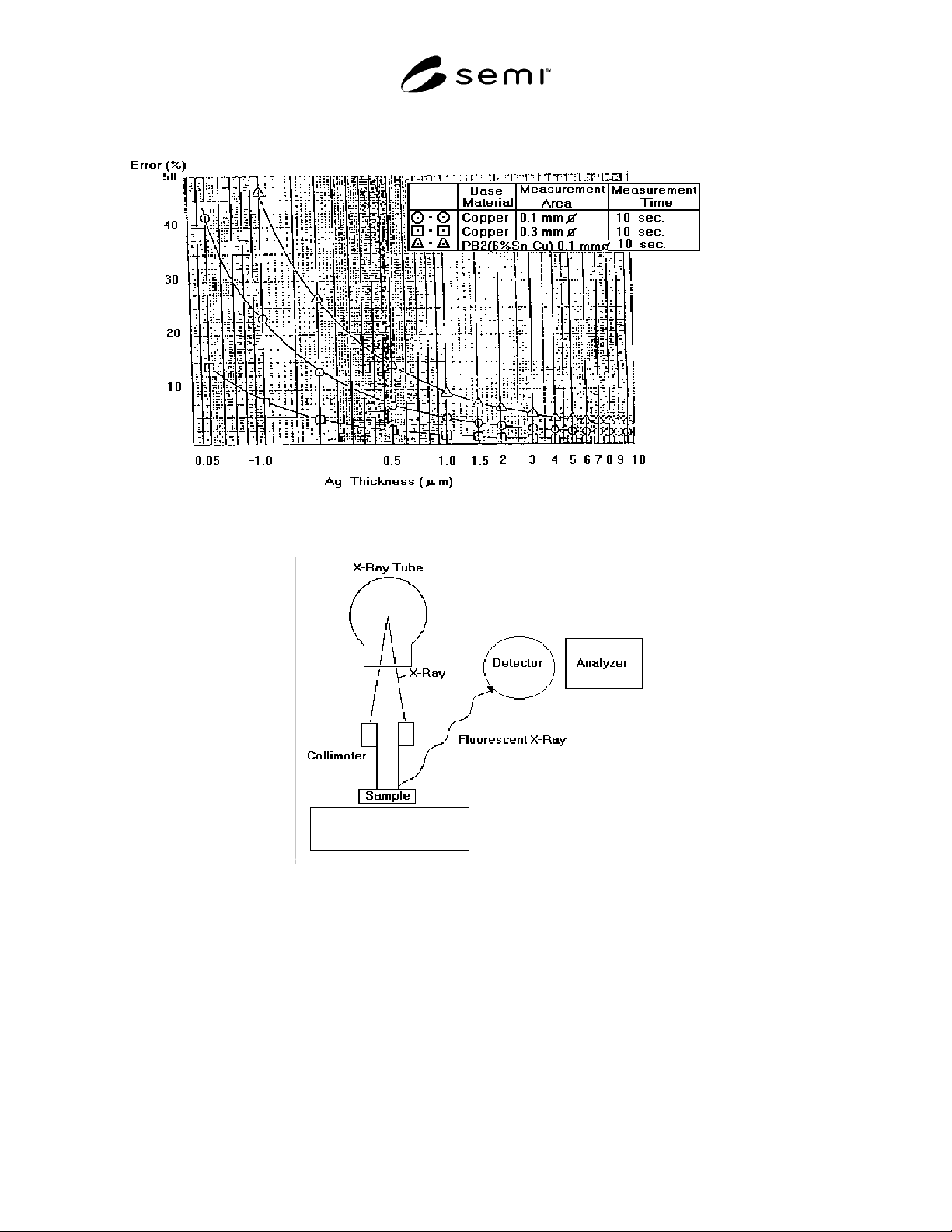
SEMI G56-93 © SEMI 1993, 2002 3 Figure 1 Error in Silver Thick ness Measurement Figure 2 Measurement Principles NOTICE: SEMI makes no warran ties o r representations as to the suitability of th e standards set forth here…
SEMI G56-93 © SEMI 1993, 2002 2
11.2 Calibration
11.2.1 Calibration curves shall be generated using
standard samples traceable to the National Institute of
Standards and Technology or equivalent standards
organization.
11.2.2 Calibration curves shall be generated after the
equipment has stabilized per the manufacturer’s
instructions.
11.2.3 The equipment shall be recalibrated every 8
hours.
12 Procedure
12.1 Procedure
12.1.1 Measurements shall be made close to the center
of the die pad, if possible. In those situations where the
die pad is not plated, the measurement site shall be
agreed between user and supplier.
12.1.2 Measure all the selected samples according to
the equipment manufacturer’s instructions.
NOTE: Refer to the equipment manufacturer’s instructions
and ASTM B 568 for safety conditions.
12.2 Results
12.2.1 Thicknesses shall be rounded to the first
decimal place.
13 Report
The report when used by a supplier to certify a user’s
requirements or by the user at incoming inspection shall
contain, at least, the following information. Other
information which is reported shall be agreed between
the user and supplier.
13.1 Supplier’s Lot Number and Date of Shipment
13.2 Test Conditions
13.3 Results from Section 11. (SPC charting
techniques may be used to monitor results for each
leadframe type and plating requirement.)
14 Accuracy and Precision
14.1 Accuracy
14.1.1 Figure 1 shows curves of silver plating
thickness measured by fluorescent X-Ray versus the
percentage error in that measurement for two collimator
settings for a constant measurement time.
15 Related Documents
15.1 SEMI Specifications
SEMI G21 — Plating Integrated Circuit Leadframes
15.2 JIS Specifications
2
JIS H8501 — Methods for Thickness Testing for
Metallic Coatings
JIS H8621 — Electroplated Coatings of Silver for
Engineering Purposes
15.3 Military and Federal Specifications
3
QQ-S-365 — General Requirements for Electro-
deposited Silver Plating
MIL-S-19550 — General Specification for
Semiconductor Devices
15.4 ISO Specifications
4
ISO-3497 — Metallic Coating Measurement of Coating
Thickness X-Ray Spectometry Methods
2 Japanese Industrial Standards, Available through the Japanese
Standards Association, 1-24, Akasaka 4-Chome, Minato-ku, Tokyo
107-8440, Japan. Telephone: 81.3.3583.8005; Fax: 81.3.3586.2014
Website: www.jsa.or.jp
3 Available through the Naval Publications and Forms Center, 5801
Tabor Avenue, Philadelphia, PA 19120-5099, USA. Telephone:
215.697.3321
4 ISO, 1 rue de Varembe, Case postale 56, CH01211 Geneva 20,
Switzerland
SEMI G56-93 © SEMI 1993, 2002 3
Figure 1
Error in Silver Thickness Measurement
Figure 2
Measurement Principles
NOTICE: SEMI makes no warranties or representations as to the suitability of the standards set forth herein for any
particular application. The determination of the suitability of the standard is solely the responsibility of the user.
Users are cautioned to refer to manufacturer’s instructions, product labels, product data sheets, and other relevant
literature respecting any materials mentioned herein. These standards are subject to change without notice.
The user’s attention is called to the possibility that compliance with this standard may require use of copyrighted
material or of an invention covered by patent rights. By publication of this standard, SEMI takes no position
respecting the validity of any patent rights or copyrights asserted in connection with any item mentioned in this
standard. Users of this standard are expressly advised that determination of any such patent rights or copyrights, and
the risk of infringement of such rights, are entirely their responsibility.
Copyright by SEMI® (Semiconductor Equipment and Materials
International), 3081 Zanker Road, San Jose, CA 95134. Reproduction o
f
the contents in whole or in part is forbidden without express writte
n
consent of SEMI.
SEMI X##-#### © SEMI 2001 1
SEMI G57-0302
GUIDE FOR STANDARDIZATION OF LEADFRAME TERMINOLOGY
This guide was technically approved by the Global Assembly and Packaging Committee and is the direct
responsibility of the Japanese Assembly and Packaging Committee. Current edition approved by the
Japanese Regional Standards Committee on November 26, 2001. Initially available on www.semi.org
December 2001; to be puiblished March 2002. Originally published in 1993.
1 Preface
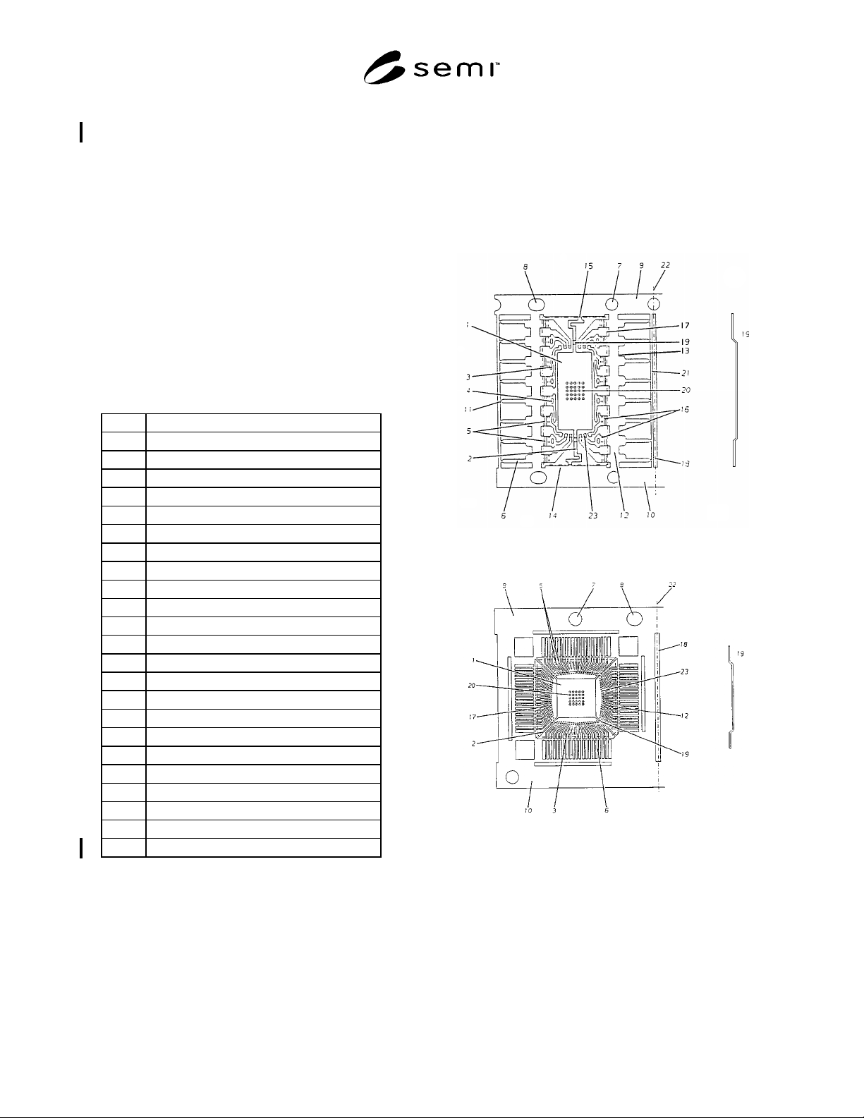
1.1 Purpose — This guideline defines standard
terminologies for all the features of leadframes used in
the production of semiconductor circuits.
1.2 Significance — Use of this guide in
communications between customers and vendors can
reduce the errors caused by the current use of different
nomenclatures for the same feature of a leadframe.
Table 1 Nomenclature for Figures
1 Die Pad
2 Die Pad Support
3 Lead Lock
4 Anchor Hole
5 Inner Lead
6 Outer Lead
7 Standard Pilot Hole
8 Pilot Hole
9 Top Rail Standard Pilot Hole Side
10 Bottom Rail
11 Lead Cut-off Notch
12 Dam Bar
13 Lead Shoulder
14 Mold Dam
15 Bumper Support Cut-off Notch
16 Lead Lock Groove
17 Mold Line
18 Expansion Slot
19 Down Set
20 Die Pad Dimple
21 Side Rail
22 Strip Cut-off Line
23 Coined Area
24 Degate Hole
Figure 1
Figure 2