semi合集-English.pdf - 第6474页
SEMI G78-0699 © SE MI 1999 7 6.6.5 If the results o f this method tu r n o ut to be unfa vora ble, the user ha s the o ptio n of ap pl ying a mor e detailed, enhanced data analysis application of this method. That appli …
SEMI G78-0699 © SEMI 1999 6
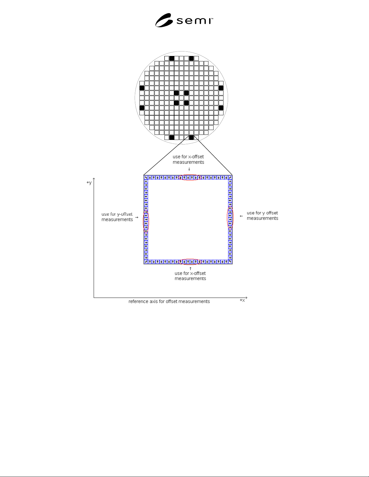
Figure 4
Recommended Dice and Pads to be used for Data Collection
6.6.3 It is important that the wafers used with this
method are probed only once, or else multiple scrub
marks may be difficult for the measurement system to
deal with and will most likely influence the analysis
results. This method assumes the wafer is ideal, having
no die skew due to wafer process anomalies.
NOTE: It is possible that a not so perfect probe tip to pad
alignment (PTTPA) may create misleading results for this
method. It is recommended that PTTPA be done on die
located at the edge of the wafer, as shown in Figure 4. This is
opposed to having PTTPA done on die in the center of the
wafer. An offset error incurred in the context of a PTTPA
done in the center may result in an incremental and continuing
error as testing moves across the wafer. With this method that
error may be averaged-out.
6.6.4 Probe system index time is device and probe
system dependent. Probe system index time is
determined by acceleration, maximum achievable
velocity, and distance traveled die to die by the chuck.
Thus, the device type chosen for use with this method
should be representative of typical die size if
meaningful index time and throughput data are to be
gathered.
SEMI G78-0699 © SEMI 19997
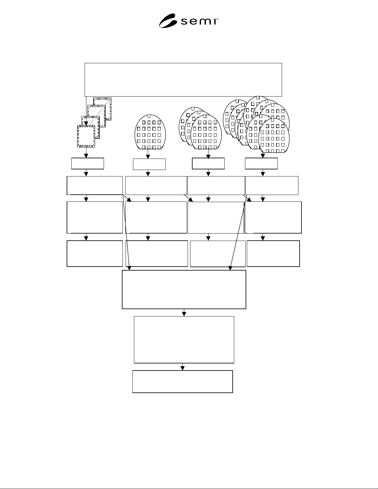
6.6.5 If the results of this method tu rn out to be
unfavorable, the user has the option of applying a more
detailed, enhanced data analysis application of this
method. That application is contained in Appendix 1.
The enhanced method uses the same data, but it
requires more manipulation of the data during data
analysis. The detail contained in the enhanced
algorithm will provide the user with greater insight as
to the cause of unfavorable results related to the probe
system under evaluation. A summary of the enhanced
method is shown in Figure 6.
6.7 Alternatives — What has been left undefined to
this point is availability of an automated approach to
data collection per the requirements of this method.
Regardless, data collection can be manually
accomplished. The manual process is laborious and
requires a video measuring system to make offset
measurements on the die pads, and a spreadsheet to
analyze the resulting data.
6.7.1 If manual operation is not desi rable or practical,
automated Probe Mark Analysis Systems do exist in the
market place as an item to be purchased. Providers are
also available to accept probed wafers and execute
probe mark analysis under contract as a service.
NOTE: A Final Note to the User of This Method — This
method provides sufficient data for sophisticated analysis of
probe system performance across die-to-die, wafer-to-wafer,
and setup-to-setup. It also provides a simple metric. It is easy
to make comparisons with simple "single number" metrics,
but that has the potential for oversight, distortion and
subsequent inappropriate comparisons. The test engineer,
working with the probe system supplier, must be the ultimate
judge of the applicability of this method and the correct
interpretation of the results.
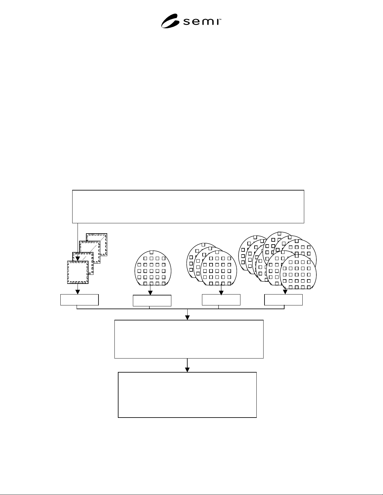
DIE
3
σ
σσ
σ
Average Die Offset
Three sigma calculation of Die Offset Values
Die to Die X and Die to Die Y variation
[REPEATABILITY]
VISION SYSTEM or PROBE MARK ANALYSIS SYSTEM
ESTABLISH
PAD OFFSETS
Offset from the center of the bond pad to the center of the scrub mark for Lot-X and Lot-Y
Average Die Offset
Average all Pad Offsets by die
(Avg. of 108 Lot-X and Avg. of 108
Lot-Y values)
SETUP LOT
1
2
WAFER
Figure 5
Pad Offset and Two-Step Analysis Algorithm for Determining Probe System Error
SEMI G78-0699 © SEMI 1999 8
DIE
Normalized Die Offset
(Normalized by Lot)
Average Die Offset - Average Lot Offset
[ACCURACY- TOTAL PROBE SYSTEM ERROR]
Three Sigma Normalized Die Offset
(Normalized by Lot)
Three sigma calculation of
Normalized Die Offset Value
[REPEATABILITY]
Three Sigma Total Probe System Error Range
Average Lot Offset +/- Total Probe System Error
VISION SYSTEM or PROBE MARK ANALYSIS SYSTEM
ESTABLISH
PAD OFFSETS
Offset from the center of the bond pad to the center of the scrub mark for all pads analyzed
Average Die Offset
Average all Pad Offsets by
die
Normalized Pad Offset
(Normalized by Die)
Pad Offset – Avg. Die
Offset
Three Sigma Normalized
Pad Offset
(Normalized by Die)
Average Wafer Offset
Avg. of Avg. Die Offset
Three Sigma Normalized
Die Offset
(Normalized by Wafer)
Normalized Die Offset
(Normalized by Wafer)
Avg. Die Offset – Avg. Wafer
Offset
Normalized Wafer Offset
(Normalized by Setup)
Avg. Wafer Offset – Avg.
Setup Offset
Three Sigma Normalized
Wafer Offset
(Normalized by Setup)
Normalized Setup Offset
(Normalized by Lot)
Avg. Setup Offset – Avg.
Lot Offset
Three Sigma Normalized
Setup Offset
(Normalized by Lot)
SETUP LOT
WAFER
1
2
Average Setup Offset
Avg. of Avg. Wafer Offset
7
3
8
4
5
6
9
Average Lot Offset
Avg. of Avg. Setup Offset
10
11
12
13
15
14
Figure 6
Pad Offsets and 15-Step Analysis Algorithm for Determining Probe System Error