semi合集-English.pdf - 第6292页
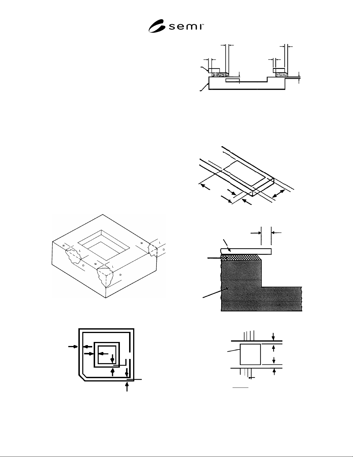
SEMI G58-94 © SEMI 1994 7 ENV S window frame base L ENV – L + Š .015 L – S 2 Figure 7 Figure 8
SEMI G58-94 © SEMI 1994 6
10 Packaging and Marking
10.1 Packaging — The shipping containers and
materials shall be suitability designed to provide the
components with protection against normal
transportation damage risks which include crushing and
spillage, and exposure to moisture and other corrosive
gases.
The packing materials must not cause particulate
contamination on the components.
10.2 Marking — The shipping container shall be
clearly marked with the following information:
Customer’s Part Number
Customer’s Purchase Order Number
Drawing Number (Customer’s and Vendor’s, if
appropriate)
Quantity
Vendor Lot Number
Shipping date
Figure 1
Chip Illustration
.010
.010
.015
.015
Figure 2
Critical and Non-Critical Seal Areas
overhang
overhang
rundown
external
pullback
window
frame
base
rundown
material
pullback
Figure 3
Glass Misalignment
.005
.015
75%
Figure 4
lead tip
overhang
lead
glass
ceramic base
Figure 5
A
B
L/F
cavity
A-B
2
Š .010 inch
Figure 6
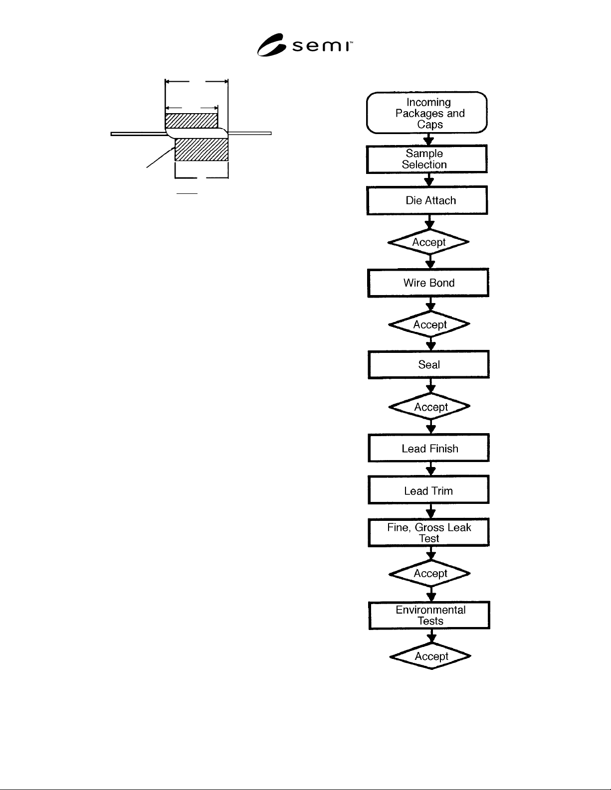
SEMI G58-94 © SEMI 19947
ENV
S
window frame
base
L
ENV – L + Š .015
L – S
2
Figure 7
Figure 8

SEMI G58-94 © SEMI 1994 8
NOTICE: These standards do not purport to address
safety issues, if any, associated with their use. It is the
responsibility of the user of these standards to establish
appropriate safety and health practices and determine
the applicability of regulatory limitations prior to use.
SEMI makes no warranties or representations as to the
suitability of the standards set forth herein for any
particular application. The determination of the
suitability of the standard is solely the responsibility of
the user. Users are cautioned to refer to manufacturer’s
instructions, product labels, product data sheets, and
other relevant literature respecting any materials
mentioned herein. These standards are subject to
change without notice.
The user’s attention is called to the possibility that
compliance with this standard may require use of
copyrighted material or of an invention covered by
patent rights. By publication of this standard, SEMI
takes no position respecting the validity of any patent
rights or copyrights asserted in connection with any
item mentioned in this standard. Users of this standard
are expressly advised that determination of any such
patent rights or copyrights, and the risk of infringement
of such rights, are entirely their responsibility.
Copyright by SEMI® (Semiconductor Equipment and Materials
International), 3081 Zanker Road, San Jose, CA 95134. Reproduction o
f
the contents in whole or in part is forbidden without express written
consent of SEMI.