semi合集-English.pdf - 第5366页
SEMI M54-0304 © SEMI 2003, 2004 7 NOTICE: SEMI makes no warranties or representatio ns as to the suitability of th e standards set forth herein for any particular application . The determinati on of the suitability o f t…
SEMI M54-0304 © SEMI 2003, 2004 6
SEMI MF523 — Standard Practice for Unaided Visual Inspection of Polished Silicon Wafer Surfaces
SEMI MF1241 — Standard Terminology of Silicon Technology
7.2 Other Docs
5
DIN 50443-2 — Testing of materials for semiconductor technology; recognition of defects and inhomogeneities in
semiconductor single crystals by X-ray topography; III-V-semiconductor compounds
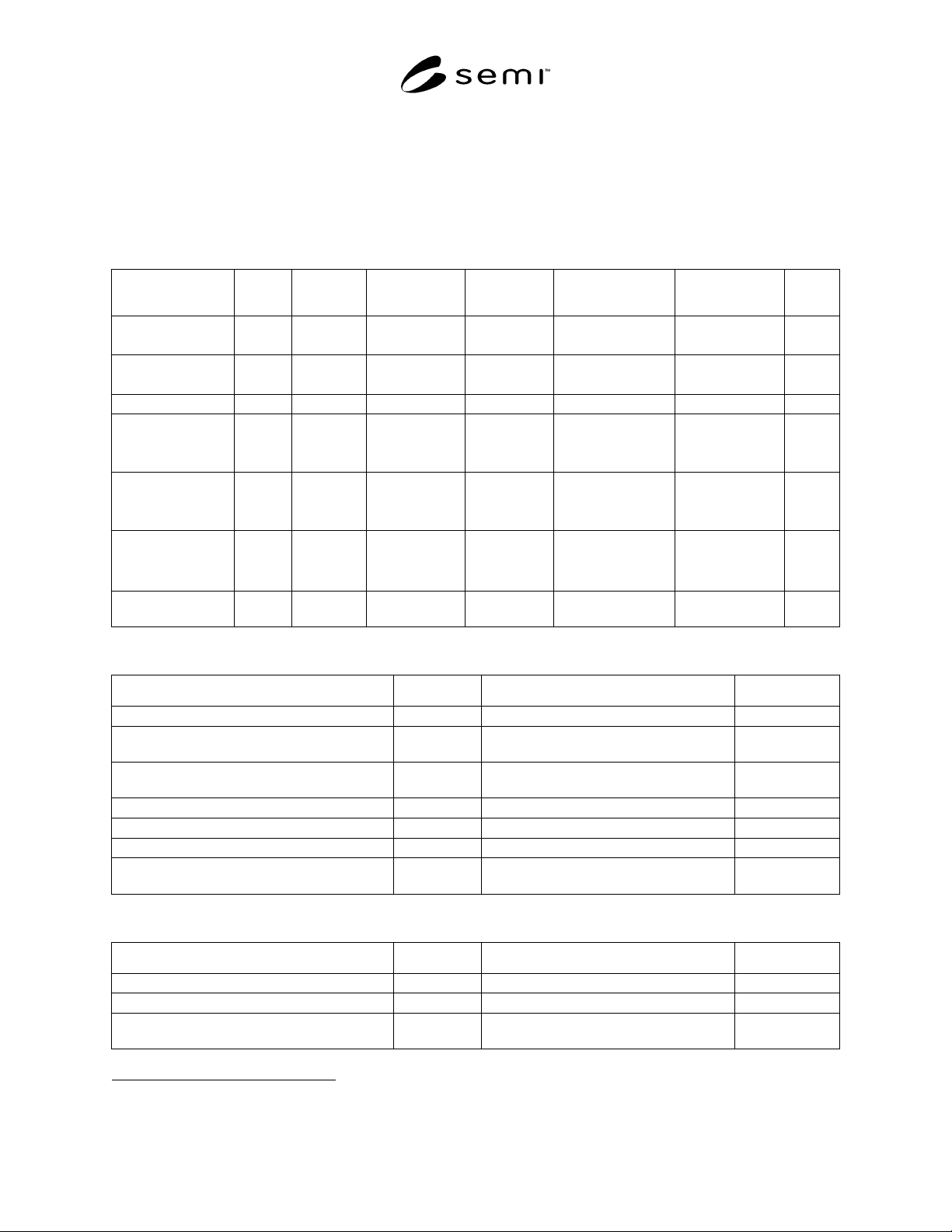
Table 1 Important SI GaAs Material Parameter Specifications and Suggested Standard Values
Parameter Section Wafer
Diameter
Suggested Value Unit Verification
Technique
Standard Test
Method
Section
Carbon
concentration
4.7 n.a. 1 × 10
15
cm
-3
LVM spectroscopy SEMI M30
DIN 50449-1
5.4
Electrical resistivity 4.11 n.a. >1 × 10
7
Ωcm
Hall effect
Capacitive probe
SEMI F76, M39
DIN 50448
5.5
Electron mobility 4.12 n.a. > 6000 cm
2
/Vs Hall effect SEMI F76, M39 5.6
EPD of LEC grown
material
4.13 150 mm
100 mm
76 mm
< 1.5 × 10
5
< 1.0 × 10
5
< 1.0 × 10
5
cm
-2
Structural etching +
light reflection
ASTM F1404,
DIN 50454-1
5.7
EPD of VGF and
VB material
4.13 150 mm
100 mm
76 mm
< 1 ×10
4
< 5 × 10
3
< 5 × 10
3
cm
-2
Structural etching,
light reflection,
microscopy
SEMI M36
DIN 50454-1
5.8
Particles with
diameter
≥ 300 nm
4.17 150 mm
100 mm
76 mm
< 100
< 40
< 20
Wafer with
edge exclusion
Laser scattering none 5.9
Microroughness
(haze)
4.17 n.a. not visible Wafer with
edge exclusion
High intensity
illumination
none 5.18
Table 2 Optional SI GaAs Material Parameter Specifications
Parameter Section Verification Technique Section
Average EL2
0
concentration 4.5 Optical absorption 5.10
Total concentration of impurities acting as
donors
4.6 GDMS, SSMS 5.11
Total concentration of impurities acting as
acceptors
4.7 GDMS, SSMS 5.12
Concentration of boron 4.9 DIN 50449-2, GDMS, SSMS, SIMS, AAS 5.13
Surface concentration of specified contaminants 4.17 TOF-SIMS, TXRF 5.14
Epi-ready qualification including shelf life 4.18 Supplier/purchaser specific 5.15
Surface irregularities (stain, scratches, pits,
orange peel, dimples)
4.17 High intensity illumination or microscopic
inspection (SEMI M15)
5.19
Table 3 Other SI GaAs Material Parameters
Parameter Section Verification Technique Section
Lateral variation of EL2
0
concentration 4.5 Optical absorption topography 5.10
Lateral variation of resistivity 4.11 Transient capacitance, DIN 50448 5.5
Lateral variation of EPD 4.14 Structural etching and light reflection, DIN
50454-1
5.8
5 Available from Deutches Institut für Normung e.V., Beuth Verlag GmbH, Burggrafenstrasse 4-10, D-10787 Berlin, Germany, website:
www.din.de

SEMI M54-0304 © SEMI 2003, 2004 7
NOTICE: SEMI makes no warranties or representations as to the suitability of the standards set forth herein for any
particular application. The determination of the suitability of the standard is solely the responsibility of the user.
Users are cautioned to refer to manufacturer' s instructions, product labels, product data sheets, and other relevant
literature, respecting any materials or equipment mentioned herein. These standards are subject to change without
notice.
By publication of this standard, Semiconductor Equipment and Materials International (SEMI) takes no position
respecting the validity of any patent rights or copyrights asserted in connection with any items mentioned in this
standard. Users of this standard are expressly advised that determination of any such patent rights or copyrights, and
the risk of infringement of such rights are entirely their own responsibility.
Copyright by SEMI® (Semiconductor Equipment and Materials
International), 3081 Zanker Road, San Jose, CA 95134. Reproduction o
f
the contents in whole or in part is forbidden without express written
consent of SEMI.
SEMI M55-0705 © SEMI 2003, 2004 1
SEMI M55-0705
SPECIFICATION FOR POLISHED MONOCRYSTALLINE SILICON
CARBIDE WAFERS
This specification was technically approved by the Global Compound Semiconductor Committee and is the
direct responsibility of the European Compound Semiconductor Materials Committee. Current edition
approved by the European Regional Standards Committee on January 8, 2003. Initially available at
www.semi.org January 2003; to be published March 2003.
NOTICE: The designation of SEMI M55 was updated during the 0705 publishing cycle to reflect the
creation of SEMI M55.2.
1 Purpose
1.1 These specifications cover substrate requirements for monocrystalline high-purity silicon carbide wafers of
crystallographic polytype 6H and 4H used in semiconductor and electronic device manufacturing.
2 Scope
2.1 A complete purchase specification may require that additional physical, electrical, and bulk properties be
defined. These properties are listed, together with test methods suitable for determining their magnitude where such
procedures are documented.
2.2 These specifications are directed specifically to silicon carbide wafers with one or both sides polished.
Unpolished wafers or wafers with epitaxial films are not covered; however, purchasers of such wafers may find
these specifications helpful in defining their requirements.
2.3 The material is Single Crystal Silicon Carbide (SiC) existing in many crystallographically different polytypes.
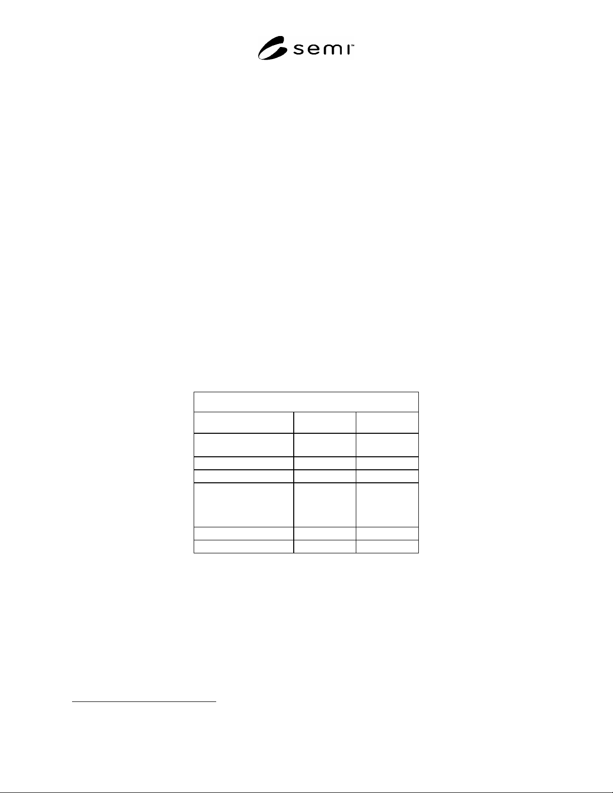
For the most common polytypes the following properties in Table 1 are listed for use as guidelines:
Table 1 Common Properties
1
Polytype 4H
6H
Lattice Parameter a
c
3.076 Å
10.053 Å
3.073 Å
15.117 Å
Stacking Sequence ABAC ABCACB
Density 3.21 g/cm
3
3.21 g/cm
3
Melting Point chemical
decomposition
above ca.
2800°C
chemical
decomposition
above ca.
2800°C
Dielectric Constant 9.7 9.7
Energy Gap 3.27 eV 3.02 eV
2.4 For referee purposes, SI (System International, commonly called metric) units shall be used.
NOTICE: This standard does not purport to address safety issues, if any, associated with its use. It is the
responsibility of the users of this standard to establish appropriate safety and health practices and determine the
applicability of regulatory or other limitations prior to use.
3 Referenced Standards
3.1 SEMI Standards
SEMI M1 Specification for Polished Mono-crystalline Silicon Wafers
1 Data as reported in Landolt-Börnstein (Springer Verlag)