semi合集-English.pdf - 第3659页
SEMI E142-0705 © SEMI 2005 21 RELATED INFORMATION 1 MAP EXAMPLES NOTICE : This rel ated inform ation is not a n official part of SEMI E142 and was derived from t he North Am erican Information & Control Committee. Th…
SEMI E142-0705 © SEMI 2005 20
APPENDIX 3
TRAY MAP ORIENTATION
NOTICE: The material in this appendix is an official part of SEMI E142 and was approved by full letter ballot
procedures on December 10, 2004.
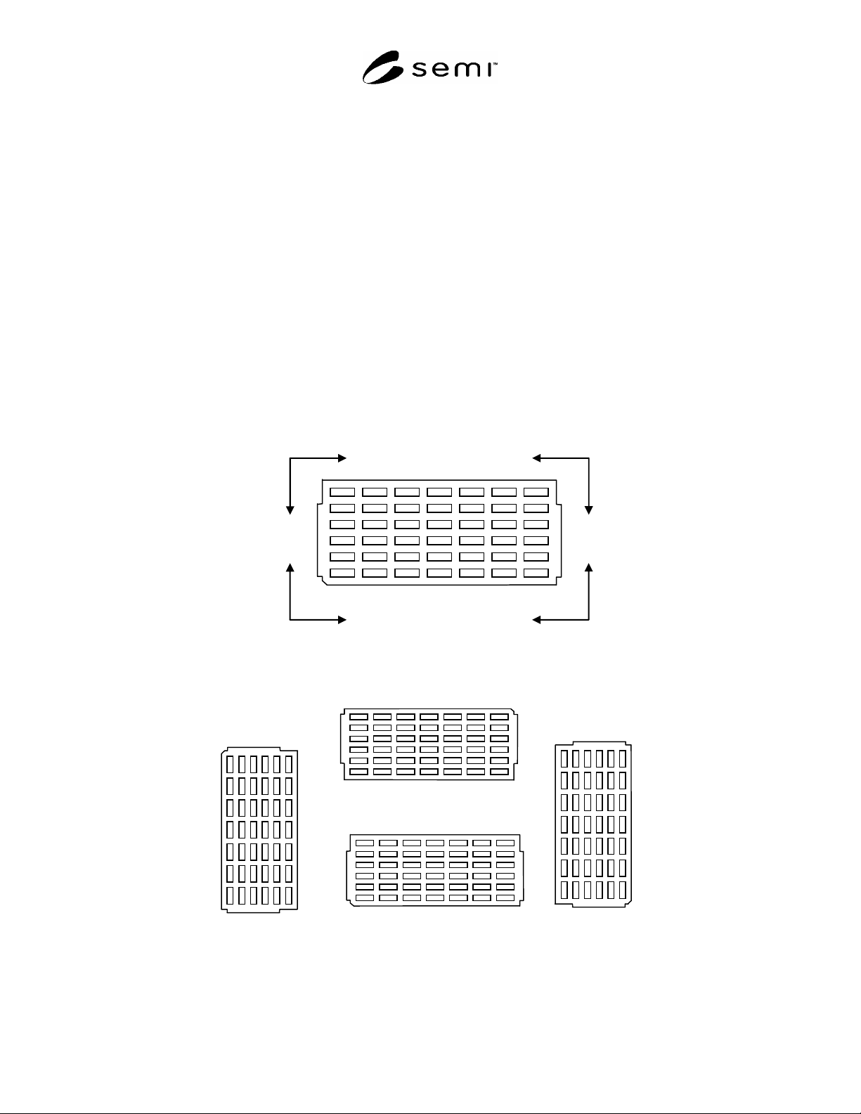
A3-1 This appendix shows how the map data items may be applied to JEDEC trays as well as some additional
information specific to this substrate type.
A3-2 The X-axis (Column) is assigned to the long axis of the JEDEC tray; the Y-axis (Row) is assigned to the short
axis of the tray. This corresponds to Cartesian coordinate “1”. For the origin of the tray, the pocket nearest the bevel
(at the bottom left corner of the tray in Figure A3-1 below) is defined as coordinate location 0,0. (Row/Column).
A3-3 The following values for OriginLocation apply to the JEDEC tray:
1 = Upper right (UR) top side
2 = Upper left (UL) top side
3 = Lower left (LL) top side
4 = Lower right (LR) top side
X
-Y
Y
-Y
Y
-X
X -X
Upper right top side
Lower right top side
Upper left top side
Lower left top side
Figure A3-1
OriginLocation
180 Deg.
270 Deg.
90 Deg.
0 Deg.
Figure A3-2
Tray Orientation

SEMI E142-0705 © SEMI 2005 21
RELATED INFORMATION 1
MAP EXAMPLES
NOTICE: This related information is not an official part of SEMI E142 and was derived from the North American
Information & Control Committee. This related information was approved for publication by full letter ballot
procedures on December 10, 2004.
R1-1 Wafer Map Example
R1-1.1 The example MapData below is for three wafers that all share the same layout. The layout includes an FDI
target, used for alignment, and an array of devices.
Wafer1 includes ReferenceDevices and BinDefinitions. Wafer2 and Wafer3 do not.
Wafer1 uses the Row/Column map representation type including null bin devices.
Wafer2 uses the Row/Column map representation type excluding null bin devices.
Wafer3 uses the Array map representation type.
Wafer4 uses the Coordinate map representation type.
<?xml version="1.0" encoding="utf-8" ?>
<MapData xmlns="urn:semi-org:xsd.4032.V0804.SubstrateMap" >
<Layouts>
<Layout LayoutId="WaferLayout" DefaultUnits="mm" TopLevel="true" >
<DeviceSize X="300" Y="300" />
<Dimension X="1" Y="1" />
<ChildLayouts>
<ChildLayout LayoutId="FDI Target" />
<ChildLayout LayoutId="Devices" />
</ChildLayouts>
</Layout>
<Layout LayoutId="FDI Target" DefaultUnits="microns" >
<Dimension X="1" Y="1" />
<LowerLeft X="0" Y="0" />
<DeviceSize X="0" Y="0" />
</Layout>
<Layout LayoutId="Devices" DefaultUnits="microns" >
<Dimension X="4" Y="3" />
<LowerLeft X="0" Y="0" />
<DeviceSize X="0" Y="0" />
<ProductId>Product1</ProductId>
</Layout>
</Layouts>
<Substrates>
<Substrate SubstrateType="Wafer" SubstrateId="Wafer1" >
<LotId>Lot1</LotId>
<AliasIds>
<AliasId Type="FrameId" Value="Frame1" />
</AliasIds>
</Substrate>
<Substrate SubstrateType="Wafer" SubstrateId="Wafer2" />
<Substrate SubstrateType="Wafer" SubstrateId="Wafer3" />
<Substrate SubstrateType="Wafer" SubstrateId="Wafer4" />
</Substrates>
<SubstrateMaps>
<SubstrateMap SubstrateType="Wafer" SubstrateId="Wafer1"
LayoutSpecifier="WaferLayout/FDI Target" >
<Overlay>
<ReferenceDevices>
<ReferenceDevice Name="FDI Target" >
<Coordinates X="0" Y="0" />
</ReferenceDevice>
</ReferenceDevices>
</Overlay>
</SubstrateMap>
<SubstrateMap SubstrateType="Wafer" SubstrateId="Wafer1"
LayoutSpecifier="WaferLayout/Devices" >
<Overlay MapName="SortGrade" MapVersion="1" >
<ReferenceDevices>
<ReferenceDevice Name="FirstDevice" >
<Coordinates X="1" Y="2" />

SEMI E142-0705 © SEMI 2005 22
</ReferenceDevice>
</ReferenceDevices>
<BinCodeMap BinType="Ascii" NullBin="." >
<BinDefinitions>
<BinDefinition BinCode="1" BinCount="5" BinQuality="Pass"
BinDescription="Tested Ok" Pick="true" />
<BinDefinition BinCode="2" BinCount="3" BinQuality="Fail"
BinDescription="Test Failed" Pick="false" />
</BinDefinitions>
<BinCode>.12.</BinCode>
<BinCode>1112</BinCode>
<BinCode>.21.</BinCode>
</BinCodeMap>
</Overlay>
</SubstrateMap>
<SubstrateMap SubstrateType="Wafer" SubstrateId="Wafer2"
LayoutSpecifier="WaferLayout/Devices" >
<Overlay MapName="SortGrade" MapVersion="1" >
<BinCodeMap BinType="Ascii" NullBin="." >
<BinCode X="1" Y="2">12</BinCode>
<BinCode X="0" Y="1">1112</BinCode>
<BinCode X="1" Y="0">21</BinCode>
</BinCodeMap>
</Overlay>
</SubstrateMap>
<SubstrateMap SubstrateType="Wafer" SubstrateId="Wafer3"
LayoutSpecifier="WaferLayout/Devices" >
<Overlay MapName="SortGrade" MapVersion="1" >
<BinCodeMap BinType="Ascii" NullBin="." >
<BinCode>.12.1112.21.</BinCode>
</BinCodeMap>
</Overlay>
</SubstrateMap>
<SubstrateMap SubstrateType="Wafer" SubstrateId="Wafer4"
LayoutSpecifier="WaferLayout/Devices"
Orientation="180" >
<Overlay MapName="SortGrade" MapVersion="1" >
<BinCodeMap BinType="Ascii" NullBin="." >
<BinCode X="1" Y="2">1</BinCode>
<BinCode X="2" Y="2">2</BinCode>
<BinCode X="0" Y="1">1</BinCode>
<BinCode X="1" Y="1">1</BinCode>
<BinCode X="2" Y="1">1</BinCode>
<BinCode X="3" Y="1">2</BinCode>
<BinCode X="1" Y="0">2</BinCode>
<BinCode X="2" Y="0">1</BinCode>
</BinCodeMap>
</Overlay>
</SubstrateMap>
</SubstrateMaps>
</MapData>
R1-2 Strip Map Example
R1-2.1 The example strip map below contains a more complex nested layout, one strip substrate, and three data
maps.
<?xml version="1.0" encoding="utf-8" ?>
<MapData xmlns="urn:semi-org:xsd.4032.V0804.SubstrateMap">
<Layouts>
<Layout LayoutId="StripLayout" DefaultUnits="100Microns" >
<Dimension X="1" Y="1" />
<DeviceSize X="2510.00" Y="414.02" />
<ChildLayouts>
<ChildLayout LayoutId="SRAM" />
</ChildLayouts>
</Layout>
<Layout LayoutId="SRAM" DefaultUnits="100Microns">
<Dimension X="10" Y="3" />
<LowerLeft X="7.00" Y="8.33" />
<DeviceSize X="75.00" Y="46.67" />
<StepSize X="78.00" Y="49.67" />
<Z Order="0" Height="500" Units="microns" />
<ChildLayouts>
<ChildLayout LayoutId="FLASH" />
</ChildLayouts>
</Layout>
<Layout LayoutId="FLASH" DefaultUnits="100Microns">