semi合集-English.pdf - 第45页
SEMI E2-93 © SEMI 1986, 2003 3 APPLICATION NOTE NOTE: The material contained in these applic ation notes is not an official part of SEMI E2 and is not mean t to modify or supersede it in an y way. Rather, these notes are…
SEMI E2-93 © SEMI 1986, 2003 2
4 Referenced Documents
SEMI M1 — Specifications for Polished
Monocrystalline Silicon Wafers
SEMI M3 — Specifications for Polished Mono-
crystalline Sapphire Substrates
SEMI M9 — Specifications for Polished Mono-
crystalline Gallium Arsenide Slices
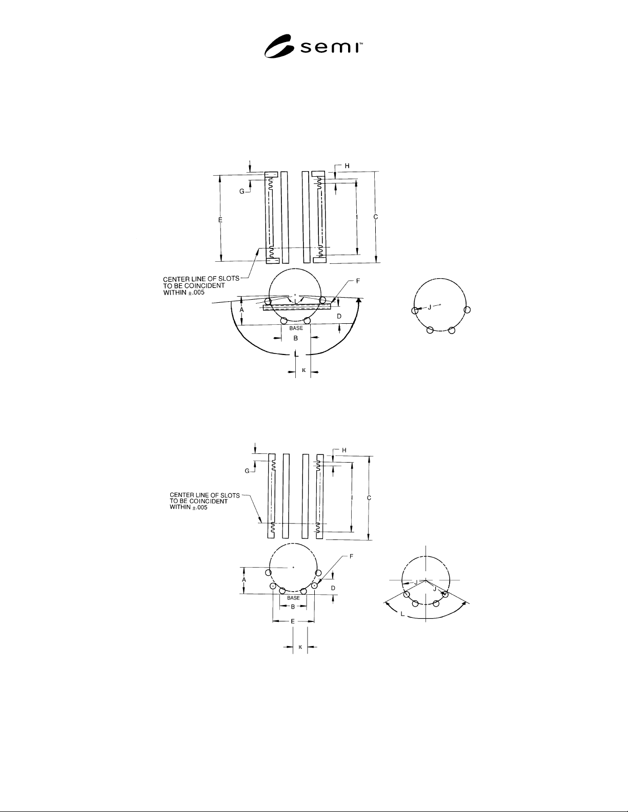
Figure 1
Style 1: Non-Contiguous 25 & 50 Slot
Figure 2
Style 2: Contiguous 25 & 50 Slot
SEMI E2-93 © SEMI 1986, 2003 3
APPLICATION NOTE
NOTE: The material contained in these application notes is not an official part of SEMI E2 and is not meant to modify or
supersede it in any way. Rather, these notes are provided primarly as a source of information to aid in the application of the
standard, as such, they are to be considered as reference material only. The standard should be referred to in all cases.
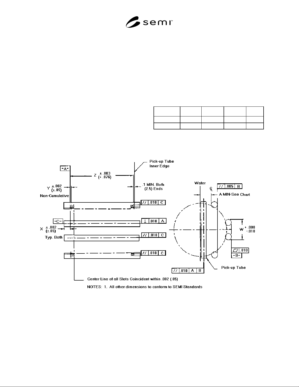
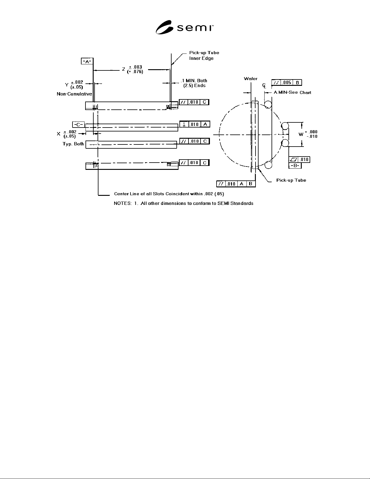
Table A1-1 lists the dimensions in linear, versus
angular, measurements for ease of dimensional
verification. The dimensions fall within SEMI
specification; however, they correspond closer to an
“L” angular dimension of 140 degrees versus the 150
degrees. The figures A1-1 and A1-2 illustrate these
dimensions for non-contiguous and contiguous style
quartz carriers.
A1-1 Carrier — Dimension L
Automated mass transfer of silicon wafers requires
edge contact below the centerline of the wafer
according to Table 1. These dimensions have been
determined as the minimum distance below the wafer
center line allowing the gripping mechanism to overlap
the vertical tangent of the wafer edge below the
centerline. This overlap allows the wafers to be
passively crattled. Contacting the wafer any higher
toward the centerline will require clamping force on the
wafers.
Table A1-1
Wafer Size 100 mm 125 mm 150 mm 200 mm
A 18 mm 21 mm 25 mm 32 mm
Style I & II (0.70" ) (0.82" ) (1.00" ) (1.25" )
Figure A1-1
Style 1: Non-Contiguous
SEMI E2-93 © SEMI 1986, 2003 4
Figure A1-2
Style 2: Contiguous
NOTICE: These standards do not purport to address safety issues, if any, associated with their use. It is the
responsibility of the user of these standards to establish appropriate safety and health practices and determine the
applicability of regulatory limitations prior to use. SEMI makes no warranties or representations as to the suitability
of the standards set forth herein for any particular application. The determination of the suitability of the standard is
solely the responsibility of the user. Users are cautioned to refer to manufacturer' s instructions, product labels,
product data sheets, and other relevant literature respecting any materials mentioned herein. These standards are
subject to change without notice.
The user' s attention is called to the possibility that compliance with this standard may require use of copyrighted
material or of an invention covered by patent rights. By publication of this standard, SEMI takes no position
respecting the validity of any patent rights or copyrights asserted in connection with any item mentioned in this
standard. Users of this standard are expressly advised that determination of any such patent rights or copyrights, and
the risk of infringement of such rights, are entirely their own responsibility.
Copyright by SEMI® (Semiconductor Equipment and Materials
International), 3081 Zanker Road, San Jose, CA 95134. Reproduction o
f
the contents in whole or in part is forbidden without express written
consent of SEMI.