semi合集-English.pdf - 第7403页
SEMI MF1527-1104 © SEMI 2003, 2004 9 8.7 Wafer Con ductivity Type and Surface Orientation — For control of four-point pr obes or for calibrating eddy current pr obes, conductivi ty type and surface orientati on do not i …
SEMI MF1527-1104 © SEMI 2003, 2004 8
point probes
5
or square-array four-point probes
7
are
available. These instruments provide for collection of
sufficient data to enable determination of the macro-
scale variation of the sheet resistance in detail adequate
for the application. Measurements should be taken in a
49-site pattern consisting of the center point and sites
on three equally spaced, concentric circles as specified
in SEMI MF1618. In this pattern the inner, middle, and
outer circles have 8, 16, and 24 sites, respectively. The
nominal diameter of the outer circle should be 38 mm
(Note 5). Procedures for measurements with square-
array four-point probes have not been standardized.
Dual-configuration sheet resistance measurements
using in-line four-point probes should be made in
accordance with SEMI MF1529. Since the thickness
correction factor is not established for dual-
configuration probes, the resistivity at each
measurement site cannot be calculated accurately.
However, provided that the wafer thickness is
sufficiently uniform, determination of the sheet
resistance is adequate for this application because
relative values are all that are required to establish the
variation.
8.5.2 Micro-scale variations in resistivity across the
surface of a wafer can be established by means of
spreading resistance measurements made in accordance
with SEMI MF525. It is especially important to
minimize such variations in material to be used as
resistivity reference wafers for spreading resistance
calibrations. Because of the high density of data points
required to obtain information on micro-scale variations
over a meaningful area, long times are required for
making these measurements.
NOTE 5: If it is desired to qualify a larger area of a wafer for
use in preparing chip sets for spreading resistance calibration,
the uniformity of both resistivity and thickness should be
determined over the larger area of the wafer. For
determinations of macro-scale radial resistivity uniformity, it
is recommended that, as a minimum, the site density used in
evaluating the central region of the wafer (see Section 8.5.1.2)
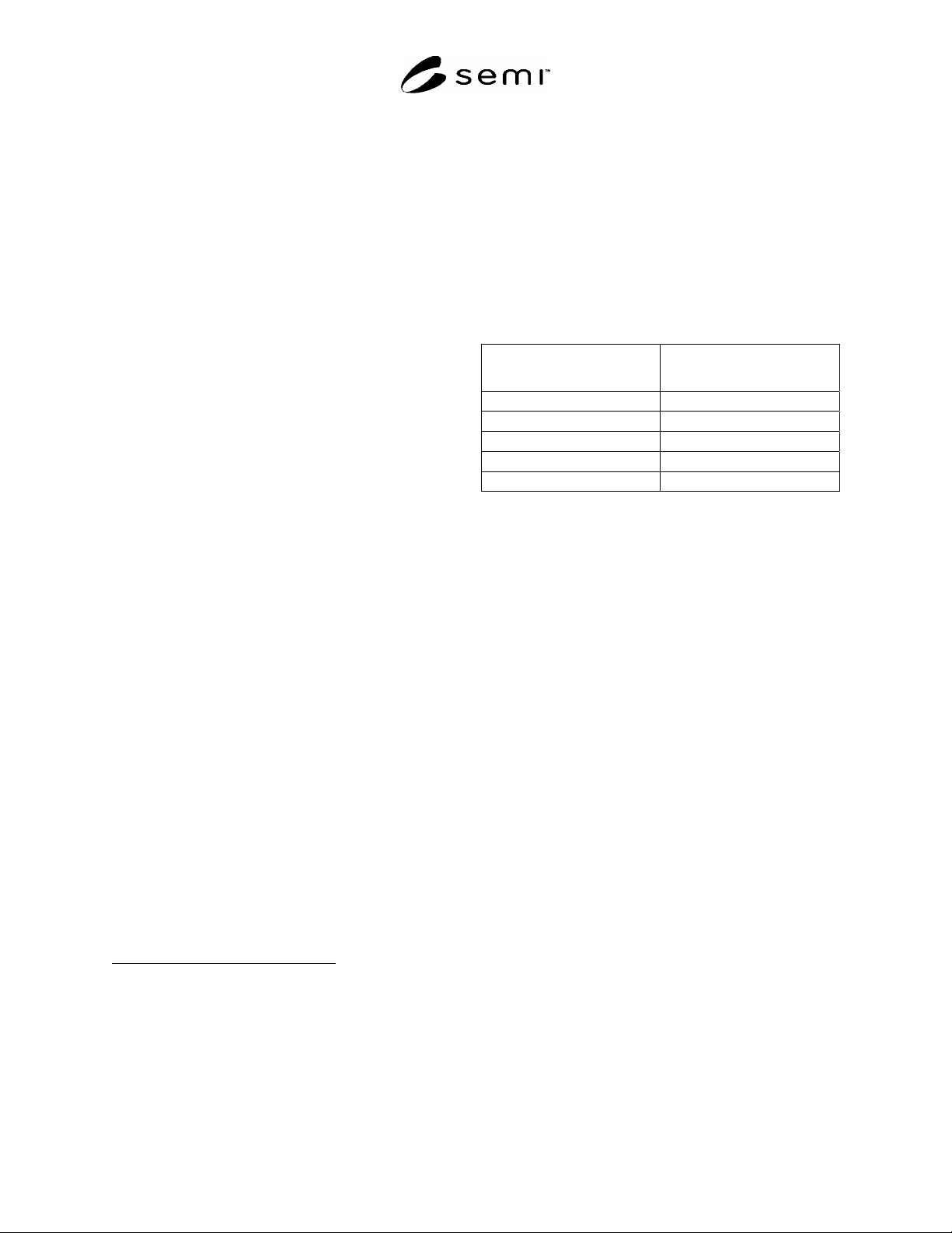
be maintained. Table 1 lists the minimum number of sites
required for areas of various diameters. Micro-scale
variations should also be determined over the larger area, but
because it is impractical to make detailed micro-scale
variation measurements on each wafer, each chip should be
evaluated for micro-scale resistivity variations prior to use.
8
7 Swartzendruber, L. J.,“Correction Factor Tables for Four-point
Probe Resistivity Measurements on Thin, Circular Semiconductor
Samples,” NBS Technical Note 199, April 1964, 42 pp. Available
from the National Technical Information Service, Springfield, VA
22161, as AD 683 408.
8 Ehrstein, J. R., “Standard Reference Materials: Preparation and
Certification of SRM's for Calibration of Spreading Resistance
Probes,” NBS Special Publication 260-93, January 1985, 30 pp.
Available from the National Technical Information Service,
Springfield, VA 22161, as PB 85-177921.
8.6 Wafer Thickness — Resistivity reference wafers
should be thick enough to avoid extreme fragility and to
allow determination of the center-point thickness to
±0.25% but not too thick to require large corrections to
the thin wafer equation for resistivity (see Section R2-
3.2). A thickness of 625 to 875 m is recommended for
resistivity reference wafers. Wafers with thickness as
small as 500 m may be used, but particular attention
must be given to control of the total thickness variation
(see Section 9.1.1).
Table 1 Minimum Number of Sites for Evaluating
Macro-Scale Resistivity Variation
Diameter of Area to be
Evaluated, mm
Minimum Number of Sites in
Map
51 81
63 121
76 169
89 225
101 289
8.6.1 For four-point probes with 1.59-mm probe-tip
spacing as specified in SEMI MF84, the thickness
correction factor is within 0.5% of unity for test
specimens up to 875-m thick. For probes with 1.016-
mm (40-mil) spacing, the thickness correction is about
1% for a test specimen thickness of 625 m, increasing
to about 5% at 875 m. For probes with 0.635-mm
(25-mil) spacing, the thickness correction is about 7.5%
at a thickness of 625 m, increasing to nearly 20% at
875 m.
8.6.2 The thickness enters into the determination of the
resistivity of the reference wafer directly as an
independent factor. Therefore determination of
thickness should be made as accurately as possible. If
manual methods are used for determining radial
resistivity uniformity (see Section 8.5.1.1), the average
thickness and total thickness variation should be
determined in accordance with the contactless method
of Test Methods SEMI MF533 using the same sites for
the thickness and resistivity measurements. This
method, however, has only marginal precision for this
application. If automated methods are used for
determining radial resistivity uniformity (see Section
8.5.1.2), the average thickness and total thickness
variation should be determined over the central 38-mm
diameter circle (Note 5) in accordance with SEMI
MF1530.
8.6.3 The various errors in resistivity determination
that result from uncertainties in thickness are discussed
in Section R2-3.2.

SEMI MF1527-1104 © SEMI 2003, 2004 9
8.7 Wafer Conductivity Type and Surface Orientation
— For control of four-point probes or for calibrating
eddy current probes, conductivity type and surface
orientation do not influence the result. In this case
these parameters should be chosen so as to provide the
most uniform specimens available. For low resistivity
reference wafers, p-type (100) or (111) wafers are most
appropriate, while for high resistivity reference wafers,
n-type (neutron transmutation doped) wafers of either
orientation are preferred. For use in calibrating
mercury probes, the conductivity type of the reference
wafers must match that of the specimens to be tested.
For use in calibrating spreading resistance instruments,
the type and surface orientation of the reference wafers
must match those of the specimens to be tested.
NOTE 6: When uniformity considerations are the dominant
issue, the following should be kept in mind. At low
resistivity, wafers cut from Cz crystal are not only more
readily available but probably have better uniformity than
wafers cut from FZ crystals. Wafers cut from MCz crystals,
if available, may be an acceptable alternative to NTD wafers
for the higher resistivity ranges. In general, (100) crystals
have better radial resistivity uniformity than (111) crystals.
Also p-type crystals have generally better radial resistivity
uniformity than n-type crystals.
9 Preparation and Calibration of Resistivity
Reference Wafers
9.1 Wafer Preparation — Wafers should be sliced
from a qualified crystal section of the desired
resistivity, diameter, conductivity type, and orientation.
The thickness of the as-cut wafers should be at least
100 m larger than the desired finished thickness to
allow for removal of 25 m from each surface during
both etching and lapping. Etching immediately after
slicing in either KOH etching solution (see Section 5.4)
or etching solution (15 + 1) (see Section 5.5) is
recommended to remove damage introduced during
slicing. Subsequent lapping with 5 to 9-m aluminum
oxide abrasive is intended to provide both control of
thickness variation and a uniform matte surface.
9.1.1 The total thickness variation (TTV) of resistivity
reference wafers should be as small as possible. As a
minimum, the reference wafers should meet the TTV
requirement of ±1 % of the center-point thickness as
specified in SEMI MF84. For 625-m thick wafers,
this would require TTV 12.5 m. In most cases, it
should be possible to obtain lapped wafers with TTV
6 m over the entire wafer and TTV 3 m (± 0.25%
of the center-point thickness) over the region of the
wafer where the resistivity uniformity is determined
(see Section 8.5.1.2). Etched or single-side polished
wafers may have somewhat larger TTV.
9.1.2 The preferred surface finish is that obtained by
lapping with 5-m alumina powder as specified in
SEMI MF84; generally similar results can be obtained
by lapping with alumina powders up to 9 m. This
surface finish was originally chosen to provide good
probe-tip and specimen-surface wear together with
sufficient smoothness to reduce probe wander.
9
However, resistivity reference wafers intended for
calibration of mercury probe and spreading resistance
instruments must be polished. On the other hand, if
polished wafers are used for four-point probe
measurements, difficulties may be encountered with
accumulated probe damage and the resultant contact
quality degradation or surface charge, or both.
However, use of instruments calibrated with lapped
resistivity reference wafers for measuring polished
wafers could result in errors because the electrical
thickness may be different for lapped and polished
wafers of the same mechanical thickness.
NOTE 7: An unpublished roughness-thickness correlation
study has shown that the electrical thickness of lapped wafers
with root-mean-square (rms) surface roughness < 0.58 m on
both sides does not differ from the mechanical thickness by
more than 2.5 m.
9.2 Calibration
9.2.1 Determine that the candidate resistivity reference
wafer meets the resistivity uniformity requirements
appropriate to the intended application or applications
(see Sections 8.1, 8.4, and 8.5).
9.2.2 Determine the resistivity of the candidate
reference wafer at its center in accordance with SEMI
MF84 except that (1) thickness should be measured in
accordance with Section 8.6.2, (2) each determination
should consist of m measurements, where 6 m 10,
taken with the wafer rotated about (360/m) deg between
each measurement, and (3) wafers with a surface finish
that results in stable, reproducible measurements may
be used. If the measurement is made on an etched or
polished surface, equivalence with the result that would
have been obtained using a lapped surface must be
demonstrated.
9.2.3 Calculate the average resistivity corrected to
23°C in accordance with SEMI MF84 and the sample
standard deviation of the six to ten individual resistivity
measurements (corrected to 23°C).
9.2.4 If the resistivity reference wafer is to be used for
calibrating a mercury probe system, convert the
temperature-corrected average resistivity value to net
carrier density using the computational method given in
9 Hargreaves, J. K., and Millard, D., “The Accuracy of Four-probe
Resistivity Measurements on Silicon,” Brit. J. Appl. Phys. 13, 231–
234 (1962).
SEMI MF1527-1104 © SEMI 2003, 2004 10
Section 7.2 (conversion from dopant density to
resistivity) of SEMI MF723, by solving the appropriate
equation given in this section for resistivity iteratively
for the net carrier density.
9.2.5 Provide the following information with the
reference wafer:
9.2.5.1 Wafer identification (including source crystal
and position therein, orientation, conductivity type, and
dopant impurity),
9.2.5.2 Date of calibration,
9.2.5.3 Calibrating laboratory and operator,
9.2.5.4 Identification of instrumentation used,
9.2.5.5 Nominal wafer diameter, in mm,
9.2.5.6 Average wafer thickness, in mm,
9.2.5.7 Total thickness variation over the 38-mm
diameter central circle, in m,
9.2.5.8 Method for determining thickness and
thickness variation,
9.2.5.9 Nominal measuring current, in mA,
9.2.5.10 Average center-point resistivity, corrected to
23°C, in ·cm,
9.2.5.11 Number of resistivity measurements (m) per
determination, and
9.2.5.12 Standard deviation of corrected center-point
resistivity values, in ·cm.
9.2.6 If appropriate for the application also provide any
or all of the following:
9.2.6.1 Net carrier density, in cm
3
,
9.2.6.2 Diameter of the area over which thickness and
radial resistivity uniformity were obtained, if different
from 38 mm,
9.2.6.3 Measures of macro-scale and micro-scale radial
sheet resistance (resistivity) uniformity, including the
method or methods by which the uniformity was
determined,
9.2.6.4 Measure of axial resistivity uniformity
estimate, including a description of the procedure by
which the estimate was obtained, and
9.2.6.5 Average voltage-current ratio, corrected to
23°C for a four-point probe with ideal (equal) 1.59-mm
probe-tip spacing.
10 Application of Resistivity Reference
Materials
10.1 Calibration procedures for various resistivity
measurement equipment are given in the applicable
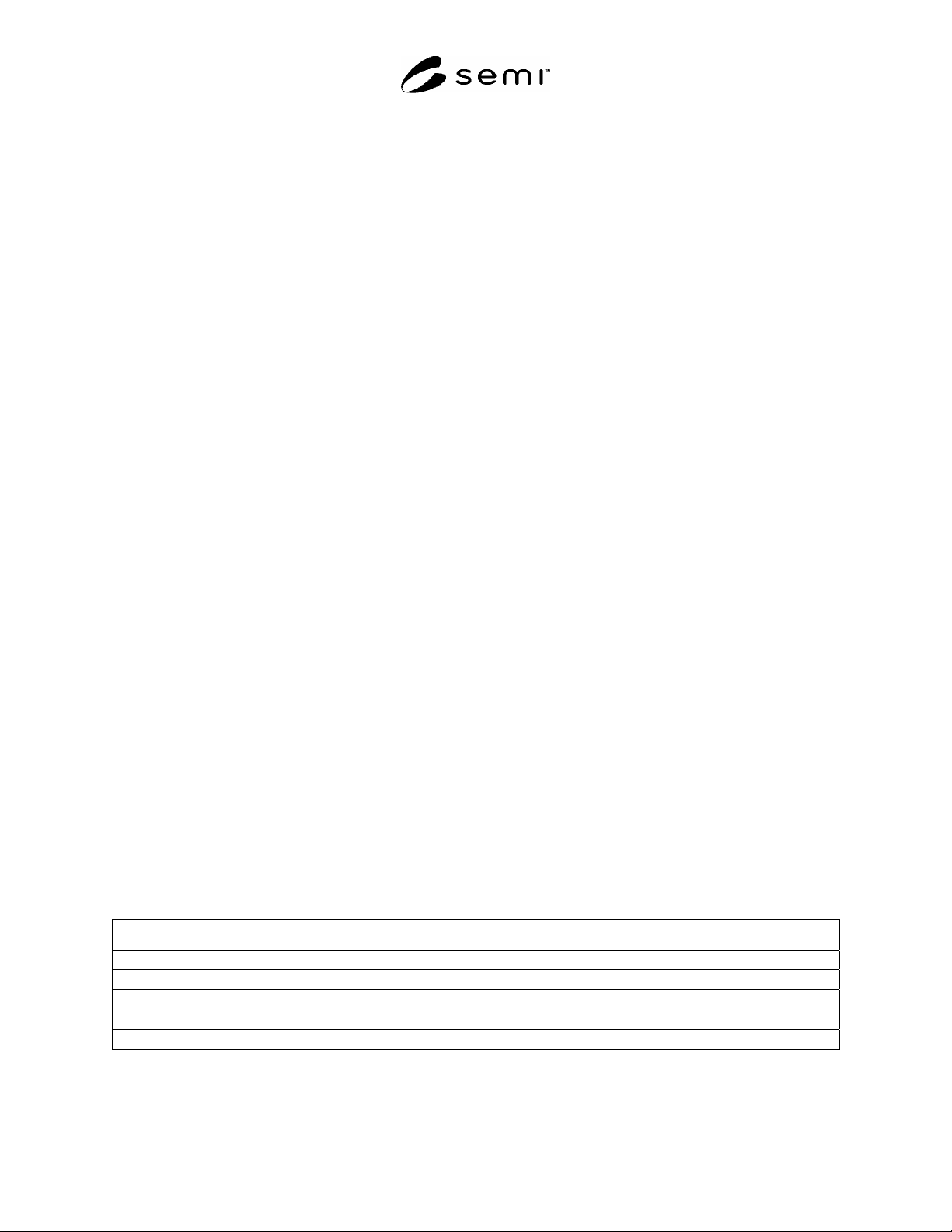
resistivity test method as summarized in Table 2.
10.2 For control of instruments for routine resistivity
measurements, a control chart for individuals with
moving range should be employed. In general, single
measurement determinations of resistivity are made for
routine purposes; therefore, the control should be
carried out on this basis. Established procedures should
be used for generating and maintaining the individuals
and moving range control charts, for determining the
existence of out-of-control conditions, and taking the
appropriate corrective action. A suggested procedure is
given in Section R1-4 for use in organizations without
previously established procedures.
11 Operator Training Requirements
11.1 Personnel responsible for selection and calibration
of resistivity reference wafers should be skilled in the
following areas:
11.1.1 Operation of four-point probe resistivity
measurement apparatus, including familiarity with
SEMI MF84 or DIN 50431,
11.1.2 Sources of radial and longitudinal resistivity
variations in silicon crystal,
11.1.3 Operation of resistivity mapping apparatus,
manual or automatic, as appropriate,
Table 2 Summary of Test Methods Applicable to Resistivity and Related Measurements
Measurement Equipment Applicable Test Method(s)
In-line Four-point Probe SEMI MF84 or DIN 50431
Non-contact Eddy-current Gage SEMI MF673, DIN 50445 or DIN 50447
Spreading Resistance Probe SEMI MF525 or SEMI MF672
Mercury Probe SEMI MF1392, SEMI MF1393 or DIN 50439
Dual-configuration Four-point Probe SEMI MF1529