semi合集-English.pdf - 第143页
SEMI E19.3-0697 © SEMI 1991, 2002 1 SEMI E19.3-0697 (Reapproved 0702) PORT STANDARD FOR MECHANI CAL INTERFACE OF WAFER CASSETTE TRANSFER, 150 mm (6 inch) PORT This standard was techni cally approved by the Global P hysic…

SEMI E19.2-0697 © SEMI 1991, 2002 2
product data sheets, and other relevant literature respecting any materials mentioned herein. These standards are
subject to change without notice.
The user’s attention is called to the possibility that compliance with this standard may require use of copyrighted
material or of an invention covered by patent rights. By publication of this standard, SEMI takes no position
respecting the validity of any patent rights or copyrights asserted in connection with any item mentioned in this
standard. Users of this standard are expressly advised that determination of any such patent rights or copyrights, and
the risk of infringement of such rights, are entirely their own responsibility.
Copyright by SEMI® (Semiconductor Equipment and Materials
International), 3081 Zanker Road, San Jose, CA 95134. Reproduction o
f
the contents in whole or in part is forbidden without express written
consent of SEMI.
SEMI E19.3-0697 © SEMI 1991, 2002 1
SEMI E19.3-0697 (Reapproved 0702)
PORT STANDARD FOR MECHANICAL INTERFACE OF WAFER
CASSETTE TRANSFER, 150 mm (6 inch) PORT
This standard was technically approved by the Global Physical Interfaces & Carriers Committee and is the
direct responsibility of the North American Physical Interfaces & Carrier Committee. Current edition
approved by the North American Regional Standards Committee on March 17, 2002. Initially available at
www.semi.org June 2002, to be published July 2002. Originally published in 1991; previously published June
1997.
The complete specification for this interface includes all general requirements of SEMI E19.
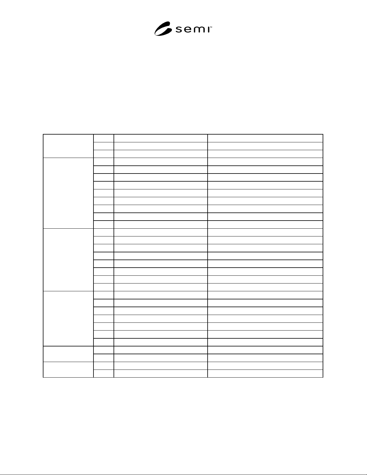
Table 1 Port Dimensions for 150 mm (6 in.) Wafer Cassette
A1 98.48 mm ± 0.13 mm (3.875 in. ± 0.005 in.)
A2 98.48 mm ± 0.13 mm (3.875 in. ± 0.005 in.)
Port Door
A3 9.53 mm ± 0.25 mm (0.375 in. ± 0.010 in.)
B1 115.57 mm ± 0.13 mm (4.550 in. ± 0.005 in.)
B2 107.95 mm ± 0.13 mm (4.250 in. ± 0.005 in.)
B3 6.35 mm ± 0.25 mm (0.250 in. ± 0.010 in.)
B4 6.35 mm ± 0.25 mm (0.250 in. ± 0.010 in.)
B5 17.78 mm (0.700 in.) maximum
B6
B7 12.70 mm (0.500 in.) minimum
B8 3.18 mm ± 0.25 mm (0.125 in. ± 0.010 in.)
Guide Rails
B9 6.35 mm (0.250 in.) maximum radius
C1 106.68 mm ± 0.13 mm (4.200 in. ± 0.005 in.)
C2 6.35 mm ± 0.13 mm (0.250 in. ± 0.005 in.)
C3 63.50 mm ± 0.13 mm (2.500 in. ± 0.005 in.)
C4 3.18 mm ± 0.05 mm (0.125 in. ± 0.002 in.) diameter
C5
C6 6.35 mm ± 0.25 mm (0.250 in. ± 0.010 in.)
C7 Full spherical radius
Latch Pins
C8 4.44 mm (0.175 in.) minimum
D1 152.40 mm ± 0.13 mm (6.000 in. ± 0.005 in.)
D2 76.20 mm ± 0.13 mm (3.000 in. ± 0.005 in.)
D3 165.10 mm ± 0.13 mm (6.500 in. ± 0.005 in.)
D4 82.55 mm ± 0.13 mm (3.250 in. ± 0.005 in.)
D5 6.35 mm ± 0.08 mm (0.250 in. ± 0.003 in.)
D6 10.16 mm ± 0.25 mm (0.400 in. ± 0.010 in.)
Registration
D7 Full spherical radius
F1 1.36 kg (3 lb) minimum Latch Pin Force each
F2 1.36 kg (3 lb) minimum
G1 12.70 mm ± 0.25 mm (0.500 in. ± 0.010 in.) Position of Cassette
G2 0.50 mm (0.020 in.) maximum
NOTICE: These standards do not purport to address safety issues, if any, associated with their use. It is the
responsibility of the user of these standards to establish appropriate safety and health practices and determine the
applicability of regulatory limitations prior to use. SEMI makes no warranties or representations as to the suitability
of the standards set forth herein for any particular application. The determination of the suitability of the standard is
solely the responsibility of the user. Users are cautioned to refer to manufacturer’s instructions, product labels,

SEMI E19.3-0697 © SEMI 1991, 2002 2
product data sheets, and other relevant literature respecting any materials mentioned herein. These standards are
subject to change without notice.
The user’s attention is called to the possibility that compliance with this standard may require use of copyrighted
material or of an invention covered by patent rights. By publication of this standard, SEMI takes no position
respecting the validity of any patent rights or copyrights asserted in connection with any item mentioned in this
standard. Users of this standard are expressly advised that determination of any such patent rights or copyrights, and
the risk of infringement of such rights, are entirely their own responsibility.
Copyright by SEMI® (Semiconductor Equipment and Materials
International), 3081 Zanker Road, San Jose, CA 95134. Reproduction o
f
the contents in whole or in part is forbidden without express written
consent of SEMI.