semi合集-English.pdf - 第7332页
SEMI MF1366-0305 © SEMI 2003, 2005 7 APPENDIX 1 ANALYSIS OF DATA FROM THE MU LTI-INSTRUMENT EXPERIMENT NOTICE : The material in this appendix is an official part of SEMI MF1366. Approval was b y full letter ballot proced…
SEMI MF1366-0305 © SEMI 2003, 2005 6
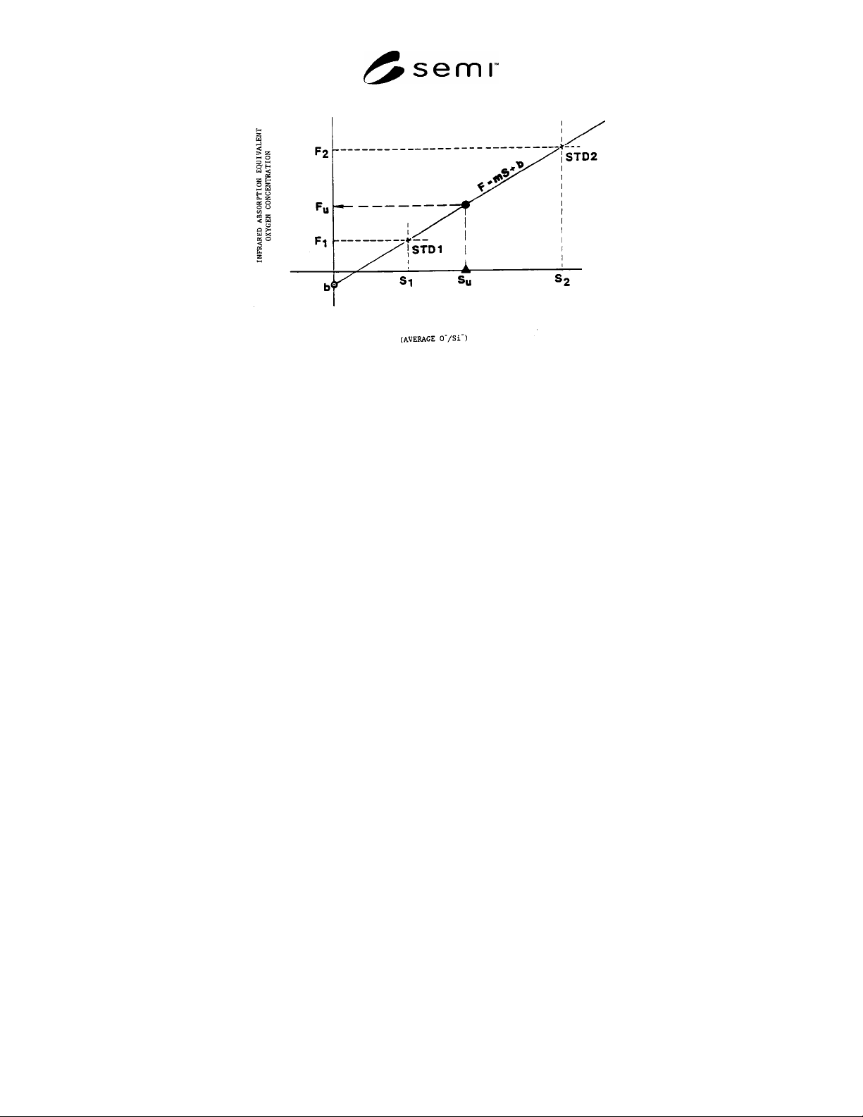
Figure 1
Load Line Calibration for SIMS Bulk Oxygen Analysis
12.2.3 Convert the SIMS O
/Si
ratios S
u
for each test specimen to the infrared absorption equivalent value F
u
by
multiplying the S
u
by the average load factor LF
avg
derived from the calibration standards, as follows:
avguu
LFSF
(5)
13 Report
13.1 Report the following information:
13.1.1 The instrument used, the operator, and the date of the measurements,
13.1.2 Identification of test and standard specimens,
13.1.3 Calibration procedure used,
13.1.4 The infrared absorption equivalent oxygen values for the test specimen and the float zone silicon specimen,
and
13.1.5 The relative standard deviations (RSD percent) of the oxygen values for the test specimen and the float zone
silicon.
14 Precision
14.1 The precision was estimated for both the load line calibration and average load factor calibration procedures
using 191 samples from one silicon wafer and measured in 191 different loads over a two-month period. The one
standard deviation was 0.38 ppma for both methods for an oxygen level of 18 ppma. The data are given in
Appendix 1.
14.2 The load line and average load line methods to quantification gave equivalent accuracy and precision in the
test outlined in ¶14.1. The reason one is used versus another is more conceptual than empirical if the oxygen values
for the standards bracket the oxygen values of the test specimens.
15 Keywords
FTIR; oxygen; secondary ion mass spectrometry; silicon
SEMI MF1366-0305 © SEMI 2003, 2005 7
APPENDIX 1
ANALYSIS OF DATA FROM THE MULTI-INSTRUMENT EXPERIMENT
NOTICE: The material in this appendix is an official part of SEMI MF1366. Approval was by full letter ballot
procedures with publication authorized by the NA Regional Standards Committee on December 10, 2004.
A1-1 The precision estimate was taken from data generated in one laboratory using three instruments and ten
instrument operators. All the instruments were CAMECA IMS 3f or 4f SIMS instruments. The test specimens were
all taken from one silicon wafer that was lightly doped and verified by infrared absorption spectroscopy to have
uniform interstitial oxygen levels across the central region where the test specimens were taken. The test specimens
were chemically mechanically polished on one side. The standards had oxygen levels that bracketed the expected
level of oxygen of the test specimen.
A1-2 The measurements were made in 191 loads over a two-month period.
A1-3 Both the load line calibration and the average load factor calibration methods were used to convert the SIMS
data to infrared absorption equivalent oxygen. The load line calibration method gave an average oxygen level of
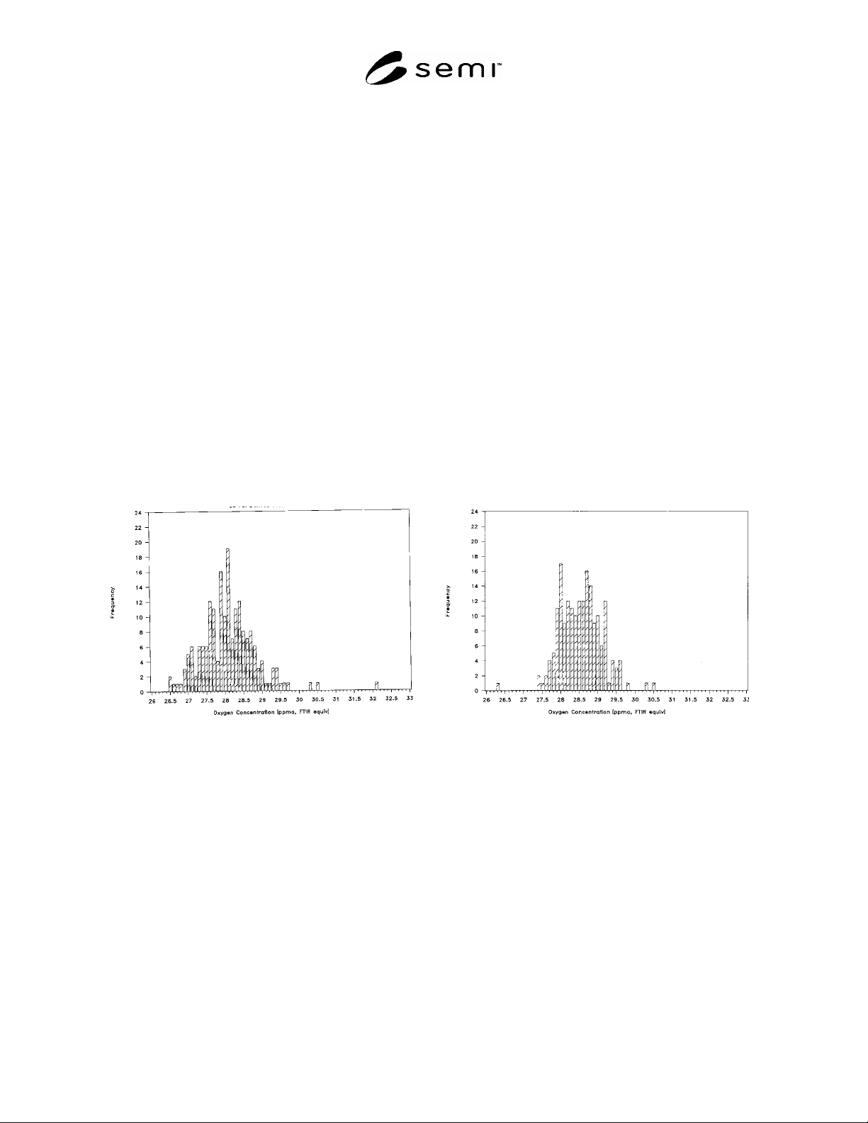
18.64 ppma (IOC-88), a one standard deviation of 0.39 ppma, and a relative standard deviation of 2.09%. A
frequency distribution is shown in Figure A1-1. The average load factor calibration method gave an average oxygen
level of 18.61 ppma (IOC-88), a one standard deviation of 0.365 ppma, and a relative standard deviation of 1.97%.
A frequency distribution is shown in Figure A1-2.
NOTE 1: The oxygen concentration scale in Figures A1-1 and A1-2 is given in Old ASTM units. These must be multiplied by
0.652 to get the values of oxygen concentration in IOC-88 units. This difference in scale arises from an historical basis and does
not affect the conclusions reached. Note also that the oxygen values in §A1-3 have been adjusted to obtain the results in IOC-88
units.
Figure A1-1
Frequency Distribution of SIMS Measured Oxygen
Using the Load Line Calibration Method
Figure A1-2
Frequency Distribution of SIMS Measured Oxygen
Using the Average Load Factor Calibration Method
NOTICE: SEMI makes no warranties or representations as to the suitability of the standards set forth herein for any
particular application. The determination of the suitability of the standard is solely the responsibility of the user.
Users are cautioned to refer to manufacturer's instructions, product labels, product data sheets, and other relevant
literature, respecting any materials or equipment mentioned herein. These standards are subject to change without
notice.
By publication of this standard, Semiconductor Equipment and Materials International (SEMI) takes no position
respecting the validity of any patent rights or copyrights asserted in connection with any items mentioned in this
standard. Users of this standard are expressly advised that determination of any such patent rights or copyrights, and
the risk of infringement of such rights are entirely their own responsibility.
Copyright by SEMI® (Semiconductor Equipment and Materials
International), 3081 Zanker Road, San Jose, CA 95134. Reproduction of
the contents in whole or in part is forbidden without express written
consent of SEMI.

SEMI MF1389-0704 © 2004 1
SEMI MF1389-0704
TEST METHODS FOR PHOTOLUMINESCENCE ANALYSIS OF SINGLE
CRYSTAL SILICON FOR III-V IMPURITIES
This guide was technically approved by the Global Silicon Wafer Committee and is the direct responsibility
of the North American Silicon Wafer Committee. Current edition approved for publication by the North
American Regional Standards Committee on March 14, 2004. Initially available at
www.semi.org
May
2004; to be published July 2004. Original edition published by ASTM International as ASTM F 1389-92.
Last previous edition SEMI MF1389-00.
1 Purpose
1.1 Electronic-grade polycrystalline silicon producers
and users require information regarding impurities for
quality assurance as well as for research and
development purposes. Polysilicon is float-zoned and a
sample from the zoned rod is analyzed following these
test methods to obtain impurity densities that can be
related to the impurity content of the starting material
(see SEMI MF1723).
1.2 Photoluminescence analysis identifies and
quantifies the electrically active dopant impurities in
monocrystalline silicon. These test methods address
boron, phosphorus, arsenic, and aluminum, found as
impurities in electronic grade silicon.
1.3 These test methods can be applied to doped and
undoped float-zoned or Czochralski material.
2 Scope
2.1 These test methods cover the simultaneous
determination of electrically active boron, phosphorus,
arsenic, and aluminum content in low-dislocation
monocrystalline silicon.
NOTE 1: These chemical species can also be determined by
the low temperature infrared analysis procedure of SEMI
MF1630.
2.2 These test methods can be used for samples that
have dopant densities between approximately 1 × 10
11
and approximately 5 × 10
15
atoms/cm
3
.
2.3 The concentrations obtained using these test
methods are based on an empirically determined
relationship of the logarithm of the concentration to the
logarithm of specific luminescence line-intensity ratios.
2.4 The empirical relationship established assumes a
constant sample excitation level for all measurements
on a given instrument.
2.5 To accommodate differences in instrumentation,
two methods are included. Test Method A refers to
procedures appropriate for dispersive infrared
spectrophotometers operating under the high sample
excitation conditions and Test Method B refers to
procedures appropriate for Fourier transform
instruments operating under low excitation conditions.
2.5.1 Typical calibration curves for each test method
are provided. These curves are modified for each
instrument using the analysis of standard samples as
reference data. Once modified, the curves for a given
instrument should produce sample dopant density
values that agree with other similarly operated
instruments using the same test method. Data obtained
using Test Method A may not agree with data obtained
using Test Method B, hence values must be reported
with reference to the test method used.
NOTE 2: Several different methods of photoluminescence
analysis are currently in practice worldwide. These test
methods address two of these, one (Test Method A) in use
primarily in Japan
1
and the other (Test Method B) primarily in
the United States. Recently published works
2,3
describe other
approaches.
2.6 Many laboratories use photoluminescence to
analyze epitaxial layers. However this application
encounters many variables and the underlying physics
is not fully understood; hence these test methods do not
attempt to outline standard practices regarding such
analysis.
NOTICE: This standard does not purport to address
safety issues, if any, associated with its use. It is the
responsibility of the user of this standard to establish
appropriate safety and health guides and determine the
applicability of regulatory or other limitations prior to
use.
1 Test Method A is essentially equivalent to JIS H 0615, Test
Method for Determination of Impurity Concentrations in Silicon
Crystal by Photoluminescence Spectroscopy. This standard is
available from Japanese Standard Association 1-24, Akasaka 4
Chome, Minato-ku, Tokyo 107-0000, Japan. Telephone: 81-(0)3-
3583-8005; Fax: 81-(0)3-3586-2014; Website:
www.jsa.or.jp
.
2 Colley, P. McL., and Lightowlers, E. C., “Calibration of the
Photoluminescence Technique for Measuring B, P, and Al Concen-
trations in Silicon in the Range 1e12 to 1e15 at/cm 3 Using Fourier
Transform Spectroscopy,” Semiconductor Science and Technology 2,
157–166 (1987).
3 Schumacher, K. L., and Whitney, R. L., J. Electron. Materials
18(6), 681–687 (1989).