semi合集-English.pdf - 第5197页
SEMI M36-0699 © SE MI 1999 1 SEMI M36-0699 TEST METHOD FOR MEA SURING ETCH PI T DENSITY (EPD) IN LOW DISLOCATION DENSITY G A LLI UM ARSENIDE WAFERS This test method was te chnically a pproved by the Globa l Compound Sem …

SEMI M35-1104 © SEMI 1999, 2004 4
Table 1 Specification Elements Related to Automatic Inspection of Silicon Wafer Surfaces
Parameter Specification Elements Specified Measurement Conditions
1. Generic LLS ___, max number with LSE dia > __nm,
nominal edge exclusion of __ mm
2. Particles ___, max number with LSE dia > __nm
nominal edge exclusion of __ mm
3. Pits ___, max number with LSE dia > __nm
nominal edge exclusion of __ mm
4. Scratches ___, max number
length >
__ m
nominal edge exclusion of __ mm
5. Generic XLS __ ppm, max with area > __ mm
2
nominal edge exclusion of __ mm
6. Haze (conditions) __ ppm, max with __ degree incident angle,
at __ nm wavelength,
at __ polarization,
over __ sr solid collection angle,
in __degree polar direction and __
degree azimuthal direction,
nominal edge exclusion of __ mm
7. Haze (instrument) __ ppm, max
(or other statistics)
with model XXX SSIS
under YYY conditions
NOTICE: SEMI makes no warranties or representations as to the suitability of the standards set forth herein for any
particular application. The determination of the suitability of the standard is solely the responsibility of the user.
Users are cautioned to refer to manufacturer's instructions, product labels, product data sheets, and other relevant
literature, respecting any materials or equipment mentioned herein. These standards are subject to change without
notice.
By publication of this standard, Semiconductor Equipment and Materials International (SEMI) takes no position
respecting the validity of any patent rights or copyrights asserted in connection with any items mentioned in this
standard. Users of this standard are expressly advised that determination of any such patent rights or copyrights, and
the risk of infringement of such rights are entirely their own responsibility.
Copyright by SEMI® (Semiconductor Equipment and Materials
International), 3081 Zanker Road, San Jose, CA 95134. Reproduction
of the contents in whole or in part is forbidden without express written
consent of SEMI.

SEMI M36-0699 © SEMI 19991
SEMI M36-0699
TEST METHOD FOR MEASURING ETCH PIT DENSITY (EPD) IN LOW
DISLOCATION DENSITY GALLIUM ARSENIDE WAFERS
This test method was technically approved by the Global Compound Semiconductor Committee and is the
direct responsibility of the Japanese Compound Semiconductor Materials Committee. Current edition
approved by the Japanese Regional Standards Committee on March 17, 1999. Initially available at
www.semi.org April 1999; to be published June 1999.
1 Purpose
1.1 This document provides a method to measure etch
pit density (EPD) in low dislocation density GaAs
wafers.
2 Scope
2.1 This test method describes a procedure to measure
EPD of 50 mm and 76 mm diameter round GaAs
wafers with an EPD of less than 5000/cm
2
.
2.2 This test method does not include GaAs wafer
preparation, such as wafer slicing, polishing and pit
etching. The preparation of GaAs wafer can be found in
a Referenced Document.
2.3 This standard does not purport to address all of the
safety issues. It is the responsibility of the user of this
standard to establish appropriate safety and health
practices and to determine the applicability of
regulations prior to use of the test method.
3 Referenced Document
3.1 ASTM Standard
F 140-92 — Test Method for Crystallographic
Perfection of Gallium Arsenide by Molten Potassium
Hydroxide (KOH) Etch Technique.
4 Apparatus
4.1 Microscope - Measuring field should be 1 mm
2
or
larger.
NOTE: For accurate EPD measurement, accurate area of the
measuring field should be measured by a standard scale.
5 Procedure
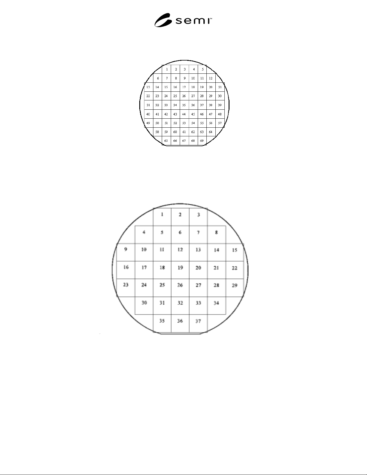
5.1 The counting positions for 50 mm diameter wafers
and for 76 mm diameter wafers are shown in Figure 1
and Figure 2 respectively. The counting points are
located in the center of each mesh. In the case of a 50
mm diameter wafer the mesh size is 5 mm. The total
number of counting positions is 69 and position 35 is
located at the center of the wafer. In the case of 76 mm
diameter wafer the mesh size is 10 mm, and the total
number of counting position is 37. Position 19 is
located at the center of the wafer.
5.2 Count and record the number of etch pits for
which the cores are in the measuring field. If the pits
are crowded and are difficult to count, increase the
magnification. After that count the etch pits and record
the results as well as the microscope magnification.
5.3 Repeat Section 5.3 for all other positions, 2
through 69 positions in the case of 50 mm diameter
wafers and 2 through 37 positions in the case of 76 mm
diameter wafers.
6 Calculations
6.1 The EPD in each measuring field is the number of
pits counted divided by the area.
EPD = (Number of pits) / Area
For example, if the size of measuring field is exactly 1
mm × 1 mm, the area is 0.01 cm
2
.
7 Report
7.1 There are several forms that are possible for
reporting the EPD, for example the average EPD of all
the positions or the area less than some specified value
or map of EPD for the entire wafer, etc. An appropriate
report form should be decided between the supplier and
the user.
SEMI M36-0699 © SEMI 1999 2
Figure 1
Counting positions for a 50 mm diameter wafer
Figure 2
Counting positions for a 76 mm diameter wafer