semi合集-English.pdf - 第6403页
APPENDIX 2 HOOK POSITION VS. PULL STRE NGTH (DEPENDENCE ON HOOK DIAMETER) NOTICE : The material in this appendix is an o fficial part of SEMI G73 and was approved by full letter b allot procedures. A2-1 Figure A2-1 NOTIC…
APPENDIX 1
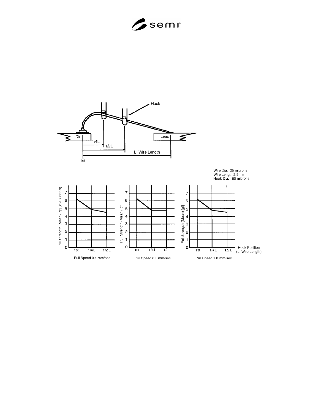
HOOK POSITION VS. PULL STRENGTH (DEPENDENCE ON PULL
SPEED)
NOTICE: The material in this appendix is an official part of SEMI G73 and was approved by full letter ballot
procedures.
A1-1
Figure A1-1
3 SEMI G73-0997 © SEMI 1997, 2004
APPENDIX 2
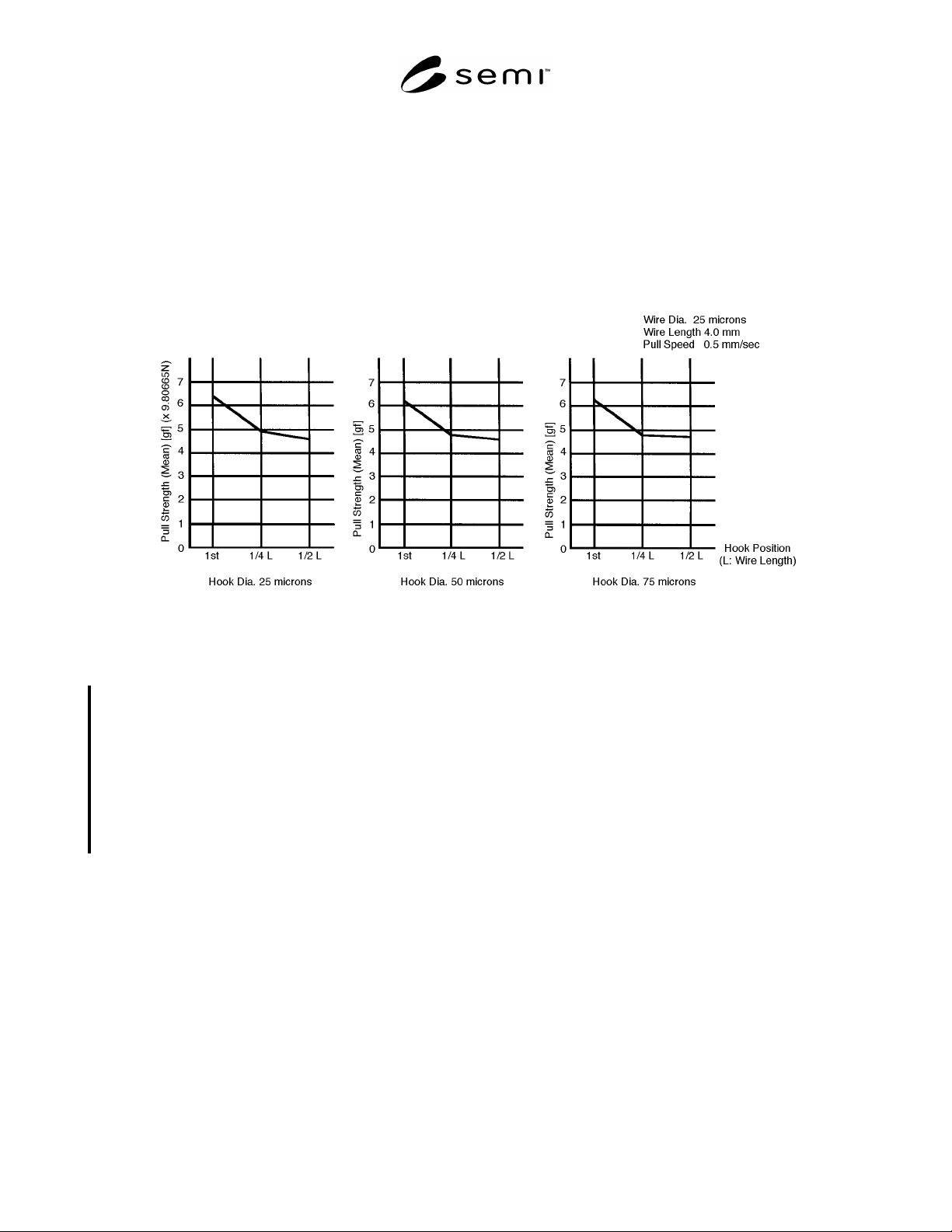
HOOK POSITION VS. PULL STRENGTH (DEPENDENCE ON HOOK
DIAMETER)
NOTICE: The material in this appendix is an official part of SEMI G73 and was approved by full letter ballot
procedures.
A2-1
Figure A2-1
NOTICE: SEMI makes no warranties or representations as to the suitability of the standard set forth herein for any
particular application. The determination of the suitability of the standard is solely the responsibility of the user.
Users are cautioned to refer to manufacturer’s instructions, product labels, product data sheets, and other relevant
literature respecting any materials or equipment mentioned herein. These standards are subject to change without
notice.
By publication of this standard, SEMI takes no position respecting the validity of any patent rights or copyrights
asserted in connection with any item mentioned in this standard. Users of this standard are expressly advised that
determination of any such patent rights or copyrights, and the risk of infringement of such rights, are entirely their
own responsibility.
SEMI G73-0997 © SEMI 1997, 2004 4
Copyright by SEMI® (Semiconductor Equipment and Materials
International), 3081 Zanker Road, San Jose, CA 95134. Reproduction of
the contents in whole or in part is forbidden without express written
consent of SEMI.
SEMI G74-0699 © SEMI 1998, 19991
SEMI G74-0699
SPECIFICATION FOR TAPE FRAME FOR 300 mm WAFERS
This specification was technically approved by the Global Assembly & Packaging Committee and is the
direct responsibility of the Japanese Packaging Committee. Current edition approved by the Japanese
Regional Standards Committee on March 17, 1999. Initially available at www.semi.org May 1999; to be
published June 1999. Originally published June 1998; previously published September 1998.
1 Purpose
1.1 The purpose of this document is to standardize the
specifications for 300 mm wafer tape frames used
between the dicing process and the die-bonding
process.
2 Scope
2.1 This standard documents the d imensions,
characteristics, and measurement methods for 300 mm
wafer tape frames.
2.2 This standard can be used as th e specification
sheet for tape frame upon purchasing.
2.3 This standard uses the SI unit system.
3 Referenced Documents
NOTE: As listed or revised, all documents cited shall be the
latest publications of adopted standards.
3.1 ANSI Standard
1
ANSI/ASME B46.1 — Surface Texture (Surface
Roughness, Waviness, and Lay)
3.2 ISO Standards
2
ISO4287 Part 1 — Surface Roughness Terminology
Part 1: Surface and Its Parameters
3.3 JIS Standards
3
JIS B0601 — Surface Roughness - Definitions and
Designations
JIS Z2245 — Method of Rockwell and Rockwell
Superficial Hardness Test
4 Terminology
4.1 tape frame — the frame which applies the wafer
tape to the wafer and retains the wafer.
1
American National Standards Institute, 1430 Broadway, New York,
NY 10018
2
International Organization for Standardization, C.P. 56, CH-1211
Geneva 20, Switzerland
3
Japanese Standards Association, 1-24, Akasaka 4 Chome, Minato-
ku, Tokyo, Japan
4.2 wafer tape — an adhesive plastic tape which
retains the wafer or diced chip. It is used between the
dicing process and the die-bonding process.
5 Ordering Information
5.1 Purchase orders for tape frames furnished to this
specification shall include quantity.
6 Requirements
6.1 Dimensions — See Table 1 and Figure 1.
Table 1 300 mm Tape Frame Dimensions
Symbol Dimension (mm
unless noted))
Note
φ A
350 ± 0.5 Inner diameter
φ B
400 ± 0.5 Outer diameter
C 380 + 0/-0.5 Width between two cords
D 380 + 0/-0.5 Width between two cords
E 170.4 Outline dimension
F 172 Outline dimension
G 86 Outline dimension
H 90 Outline dimension
I 120°
J 60° Partition out with diameter N as
standard
tK 1.5 or (1.2) Plate thickness
L 190
M 190 Frame warpage
φ N
3.2 Pin diameter
P 100 ± 0.2 Diameter N position
Q 18 ± 0.2 Diameter N position
R 276 1 Notch position
S 19.6 ± 0.2 1 Notch position
NOTE 1: Plate thickness of 1.5 mm is recommended.
NOTE 2: No burrings on the edges.
NOTE 3: Surface Roughness: R
max
≤ 1 µm, R
a
≤ 0.1 µm;
(surface indicated as ∆) unindicated Cut Surface Roughness:
R
max
≤ 100 µm, R
a
≤ 25 µm.