semi合集-English.pdf - 第552页
SEMI E78-1102 © SEMI 1998, 2002 10 recommendati on (Table 1 in Section 12.5) – 50 nanocoulom bs. A1-2.1.4 .3 Level 2 — Devices are damaged by l ower levels of stati c charge in equi pment. Devices pas s testing at MM Cla…

SEMI E78-1102 © SEMI 1998, 2002 9
APPENDIX 1
DETERMINING STATIC SENSITIVITY LEVELS
NOTE: This appendix was approved as an official part of SEMI E78 by full letter ballot procedure. This appendix offers
information related to the Sensitivity Levels contained in Section 12.5.
A1-1 Recommended Levels
A1-1.1 The recommended charge and electrostatic
field levels in this guide are not based on specific
protection thresholds for individual devices or process
tools. Rather, their aim is to classify the types of ESD
events or static levels that are likely to be of concern.
Tool manufacturers and users should determine the type
of events that are of most concern to their products and
process, so as to apply this guide to their needs.
Information on specific device damage thresholds and
tool sensitivities is best determined on an individual
basis.
A1-2 Justification of Guide Recommendations
in Section 12.5 and Table 1
A1-2.1 Recommendations for ESD Damage
A1-2.1.1 Related Information R1-1 discusses test
methods for determining ESD damage thresholds for
semiconductor devices. Devices are qualified according
to the highest ESD stresses they can withstand without
measurable change in their operating parameters. This
section attempts to develop guide recommendations for
minimizing ESD damage based on that discussion.
A1-2.1.2 Industry Device Damage Levels — Each of
the test methods, HBM, MM, and CDM have a set of
qualification levels defined. These are contained below.
HBM Classification Levels
Class Voltage
0 < 250
1A 250–499
1B 500–999
1C 1000–1999
2 2000–3999
3A 4000–7999
3B ≥ 8000
MM Classification Levels
Class Voltage
M1 < 100
M2 100–199
M3 200–399
M4 ≥ 400
CDM Classification Levels
Class Voltage
C1 < 125
C2 125–249
C3 250–499
C4 500–999
C5 1000–1499
C6 1500–1999
C7 ≥ 2000
A1-2.1.3 Charge Levels for ESD Damage — As
discussed in Related Information R1-1.4, ESD
Simulator testing uses different capacitances for each
model. For HBM it is 100 picofarads, for MM it is 200
picofarads, and for CDM it depends on the capacitance
of the actual device being tested. In any case, it is
charge (charge = voltage × capacitance) that damages
the device. It would seem appropriate, therefore, that
the guide recommendations in Table 1 Section 12.5 be
stated in units of charges (e.g. nanocoulombs).
A1-2.1.4 Guide Recommendations — Based on
industry testing reflected in device data sheets, there
appears to be a wide range for ESD immunity in
semiconductor devices. This document deals primarily
with ESD occurring within equipment. HBM type ESD
discharges are the least likely to occur within
equipment. Charged equipment parts contacting devices
(MM) and charged devices contacting machine parts
(CDM) are the most likely causes of ESD damage to
devices in equipment. The following sensitivity levels
are defined with respect to the existing industry MM
and CDM classifications.
A1-2.1.4.1 Level 4 — Devices are essentially
unaffected by any reasonable level of ESD encountered
in equipment. Devices pass testing at levels higher than
MM Class M4 (400 volts × 200 picofarads = 80
nanocoulombs). Equipment should not create or store
charge on itself or on devices in excess of the guide
recommendation. Guide recommendation (table 1 in
Section 12.5) – 100 nanocoulombs.
A1-2.1.4.2 Level 3 — Devices are affected by
moderate levels of static charge in equipment. Devices
pass testing for MM Class M4 (400 V × 200 picofarads
= 80 nanocoulombs) and most of MM Class M3 (over
250 volts × 200 picofarads = 50 nanocoulombs). Guide
SEMI E78-1102 © SEMI 1998, 2002 10
recommendation (Table 1 in Section 12.5) – 50
nanocoulombs.
A1-2.1.4.3 Level 2 — Devices are damaged by lower
levels of static charge in equipment. Devices pass
testing at MM Class M1 (100 V × 200 picofarads = 20
nanocoulombs) and CDM Class C4 (1 kV × 10
picofarad device = 10 nanocoulombs). Guide
recommendation (Table 1 in Section 12.5) – 10
nanocoulombs.
A1-2.1.4.4 Level 1 — Devices are easily damaged by
even low levels of static charge in equipment. Devices
pass testing at CDM Class 1 (125 V × 10 picofarads
device = 1.25 nanocoulombs). In most cases simulator
equipment is not designed to do testing at these very
low levels for MM. Guide recommendation (Table 1 in
Section 12.5) – 1 nanocoulombs.
A1-2.2 Recommendations for Particle Deposition
A1-2.2.1 Related Information R1-2 discusses the
enhancement of particle deposition due to electrostatic
fields from charges on the wafer surface. This section
attempts to develop the guideline recommendations for
minimizing particle deposition based on that discussion.
A1-2.2.1.1 From Equation 3 of Related Information
R1-2.2,
N
/
A = cv
elect
t (12)
where N/A equals the particulate burden added to a
wafer during exposure time t, exposed to a particle
concentration c, in an environment characterized by an
electrostatic particle deposition velocity, v
elect
.
A1-2.2.1.2 Target values for N/A are given in the
National Technology Roadmap for Semiconductors
(NTRS, 1994). These target values vary from 0.02–0.01
defects/cm
2
, depending on the critical dimensions of the
technology, and represent an upper value of the
acceptable particulate concentration on a wafer at the
conclusion of the fabrication sequence. For individual
processing steps making up the fabrication sequence the
target values are lower yet.
A1-2.2.1.3 The variables c and t are process step
dependent and may or may not be controllable. Clearly
minimizing both of these variables is desirable in order
to minimize particle deposition on a wafer in any
environment.
A1-2.2.1.4 The only variable in Equation 12 that
depends on electrical forces is v
elect
. Both the particle
charge and the electric field in the vicinity of the wafer
affect the magnitude of v
elect
. Particle charge is
generally unknown unless it is deliberately controlled
by a neutralizing action, such as flooding the
environment with both positive and negative charges.
Under these conditions a Fuchs type charge distribution
is a reasonable assumption for the particle charge. This
assumption was used to calculate the values of E
0
in
Table R1-2 of Related Information R1-2.3.2.
A1-2.2.1.5 When the environmental electric field is
less than E
0
, deposition of electrically “neutralized”
particles is dominated by diffusion. When the
environmental electric field is greater than E
0
,
electrostatic forces dominate particle deposition even
when particle charge has been “neutralized.” Values of
E
0
for a Fuchs charge distribution can be calculated
from Related Information R1-2.3.2 Equation 10. For
particle charge greater than the Fuchs charge, v
elect
increases by a factor of q/q
Fuchs
. Unfortunately, the
actual particle charge q is generally unknown.
A1-2.2.1.6 Using the process step values of c and t and
the value of v
elect
calculated from Equation 10, the value
of N/A for any process step can be estimated.
Alternatively, having a target value of N/A and
estimating the value of v
elect
as outlined in the previous
paragraphs, allows one to calculate the tolerable value
of ct:
ct =[
N
/
A]
/
v
elect
(13)
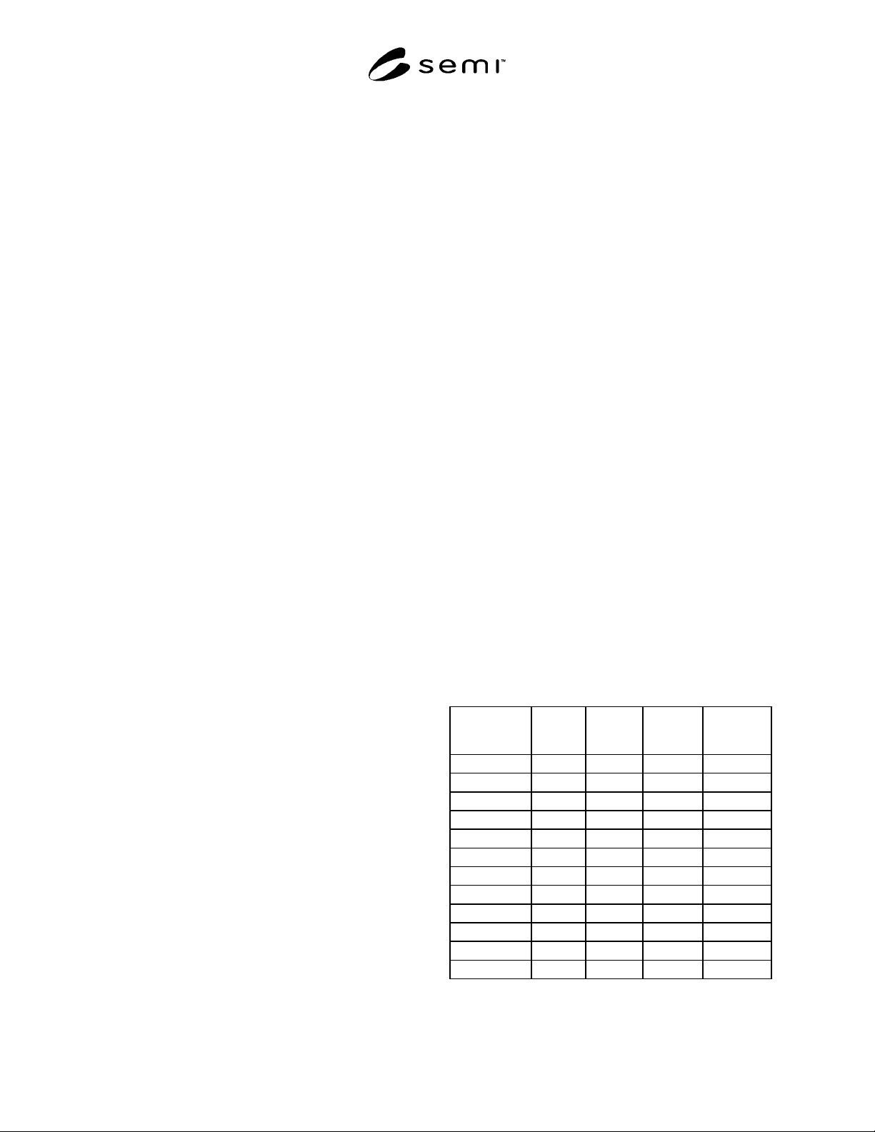
A1-2.2.1.7 Setting N/A = 0.01/cm
2
and using Equation
10 to calculate v
elect
for a 0.1 µm particle at various
values of electric field and particle charge, target values
of ct can be calculated from Equation 13. The allowed
exposure times in an ISO Class 1 environment (c ≤ 10
-5
particles/cm
3
) can be deduced as shown in the
following table:
Table A1-1 Allowed Exposure Times in an ISO
Class 1 Environment
E V/cm at One
Wafer Radius
q/q
Fuchs
v
elect
cm/sec
ct sec/cm
3
max t in ISO
Class 1 sec
4000 1 0.8 0.01250 1250
2 1.6 0.00625 625
10 8.0 0.00125 125
400 1 0.08 0.1250 12500
2 0.16 0.0625 6250
10 0.8 0.0125 1250
200 1 0.04 0.250 25000
2 0.08 0.125 12500
10 0.4 0.025 2500
100 1 0.02 0.50 50000
2 0.04 0.25 25000
10 0.2 0.05 5000
SEMI E78-1102 © SEMI 1998, 2002 11
A1-2.2.1.8 Using higher values of N/A in Equation 13
will increase the acceptable values of ct and max t.
Accepting higher values of c will reduce max t. The
guideline table provides an order of magnitude
assessment of the degree of electric field and charge
control needed in specific operations. Minimum field
and minimum particle charge are always the goal but
usually not practically achievable. This guideline table
provides background estimates of envelopes for
acceptable operation in electrically charged
environments.
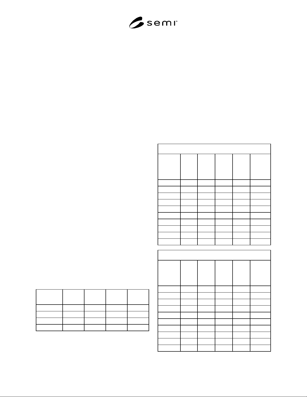
A1-2.2.2 The following simplified table is offered as
an alternative to Table A1-2 based on the following
assumptions:
1. Calculations made for Federal Standard 209E Class
1 (c ≤ 0.00124 particles/cm
3
).
2. The value of the electrostatic field is referenced at a
distance of one wafer radius from the wafer. While
electrostatic field measurements can certainly be
made at this distance, they are typically made at 2.5
cm (1 inch) with common instrumentation. This is
described in SEMI E43. Measurements made at this
smaller distance will be proportionally higher, but
under varying measurement conditions, it is difficult
to determine a precise relationship between electric
field and measurement distance. To provide a
suitable safety factor, assume a linear relationship,
rather than one proportional to the square of the
distance. For example, with a 200 mm wafer, 4000
Volts/cm at 2.5 cm would result in 1000 Volts/cm at
10 cm, rather than 250 Volts/cm.
3. The proportionality effect of q/q
Fuchs
has been
explained, as has the difficulty in actually
determining any value for it. For simplicity, the
table includes only the q = q
Fuchs
condition.
4. N/A = 0.016 defects/cm
2
as specified for 0.25 µm
technology in the National Technology Roadmap
for Semiconductors.
Table A1-2.1 Alternative to Allowed Exposure Times
in an ISO Class 1 Environment
EV/cm at 2.5
cm
N
/A defects
per cm
2
v
elect
cm/sec
ct
sec/cm
3
max t in
Class 1 sec
4000 0.016 0.21 0.0762 61
400 0.016 0.021 0.762 610
200 0.016 0.0105 1.524 1220
100 0.016 0.00525 3.048 2440
A1-2.3 Guide Recommendations for Equipment
Malfunctions
A1-2.3.1 Equipment Survey — Most semiconductor
production equipment should comply with the ESD
immunity requirements of the European Economic
Community (EEC). The testing mandated by the EEC
uses the test methods and ESD immunity levels
specified in IEC 6100-4-2. A recent survey of 262
semiconductor equipment suppliers revealed that 71%
were compliant with the EEC requirements. There is an
expectation that all equipment to be used in future 300
mm wafer fabrication will meet or exceed the ESD
immunity requirements of IEC 6100-4-2.
A1-2.3.1.1 To test for compliance, measurements were
made with the ESD simulator described by IEC 6100-4-
2 on a representative sample of semiconductor
equipment. The results were as follows:
ESD Simulator Testing Direct Contact Discharge
Equipment
Test
Voltage
Level 1
(2 kV)
Test
Voltage
Level 2
(4 kV)
Test
Voltage
Level 3
(6 kV)
Test
Voltage
Level 4
(8 kV)
Test
Voltage
Level X
(NOTE 1)
A X
B X
C X
D X
E X
F X
G X
H X
I X
J X
ESD Simulator TestingAir Discharge at 10 cm
Equipment Test
Voltage
Level 1
(2 kV)
Test
Voltage
Level 2
(4 kV)
Test
Voltage
Level 3
(8 kV)
Test
Voltage
Level 4
(15 kV)
Test
Voltage
Level X
(NOTE 1)
A X
B X
C X
D X
E X
F X
G X
H X
I X
J X