semi合集-English.pdf - 第6333页
SEMI G65-96 © SEMI 1996, 2004 6 10 Sample Preparation 10.1 The sam ples are prepared by etching a leadframe pattern into a blank piece of the lea d frame material using a standard m ask. An example of the rec ommended co…
5 SEMI G65-96 © SEMI 1996, 2004
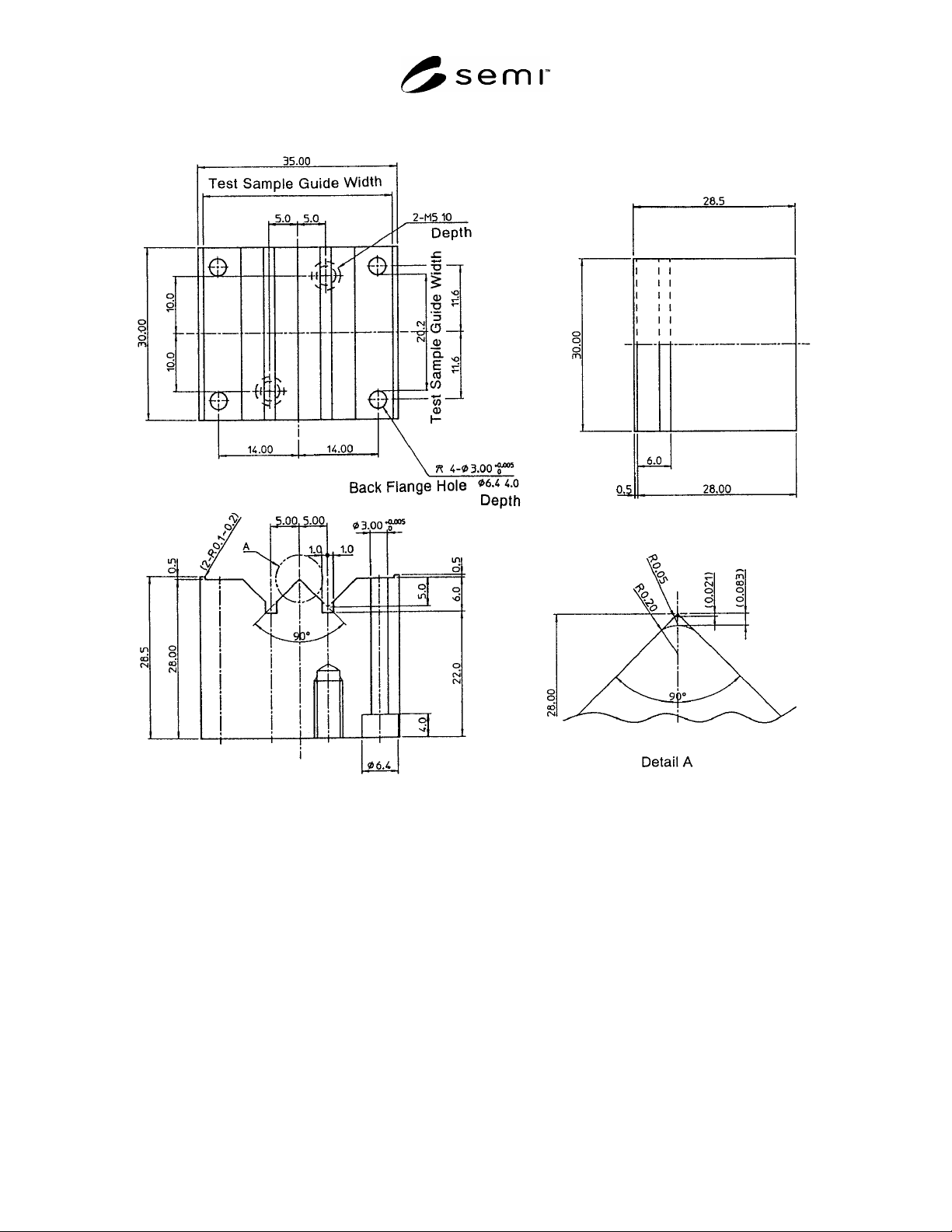
Figure 7
Die Core Detail
8.3 Micrometer
8.4 Microscope — 75× used to inspect lead surface characteristics.
8.5 Protractor — 10× and accuracy 0.1° used to measure the leadform spring back.
8.6 Projector — 10×.
9 Sampling Plan
9.1 The sampling plan shall be agreed between user and supplier. It is suggested that a minimum of five (5) samples
(2 leads per sample) of 0.3 mm width on 0.65 mm pitch, be used for these tests.
NOTE 3: If the leadframe is four-sided, take samples from both orthogonal directions.
SEMI G65-96 © SEMI 1996, 2004 6
10 Sample Preparation
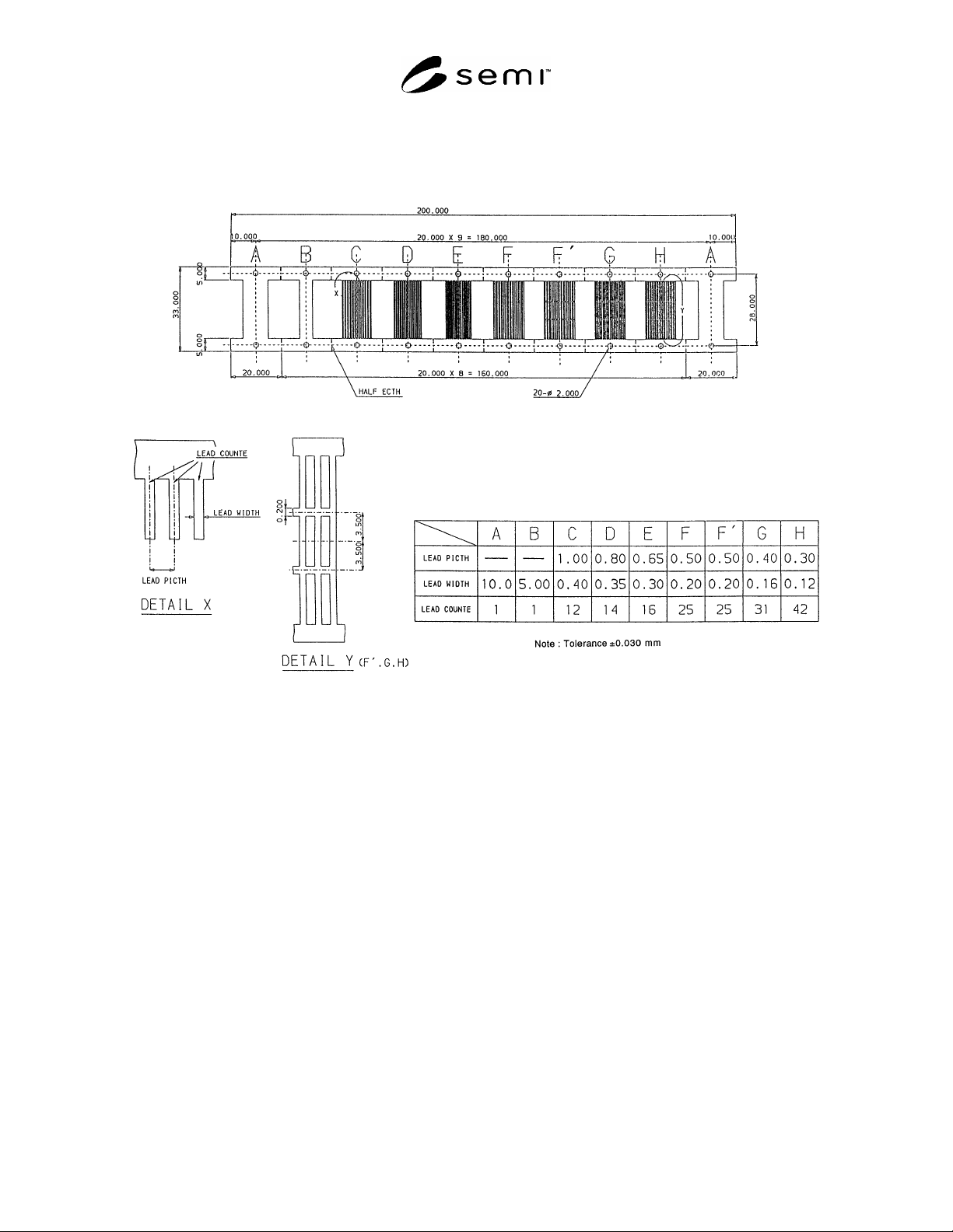
10.1 The samples are prepared by etching a leadframe pattern into a blank piece of the leadframe material using a
standard mask. An example of the recommended configuration is shown in Figure 8.
Figure 8
Standard Sample Configuration
10.2 Measure the sample thickness at three (3) points on the siderail using micrometer.
11 Setup and Procedure
11.1 Setup
11.1.1 Warm up and calibrate the tensile tester according to the operation manual.
11.1.2 Set the “W” forming tool in the tensile tester.
11.1.3 Set the tensile tester in the push mode and adjust the force to 9800N.
11.2 Procedure
11.2.1 Place the sample on the lower section of the “W” forming tool.
11.2.2 Lower the upper section of the “W” forming tool at the speed of 1 to 5 mm/min.
11.2.3 Raise up the upper section of the “W” forming tool and remove the sample carefully.
11.2.4 Repeat the test for the other samples.
11.3 Measurement
11.3.1 Remove the leads from the bent sample by cutting at the cutting position.

7 SEMI G65-96 © SEMI 1996, 2004
NOTE 4: Perform this operation carefully to avoid reforming
the leads.
11.3.2 Select two (2) leads from one sample.
11.3.3 Observe the outside surface of the lead and take
a photograph with a microscope set at 75×
magnification.
11.3.4 Set the lead sample in a projector.
11.3.5 Project the picture of the sample on the screen.
11.3.6 Adjust the protractor to the picture and read the
form angle.
12 Calculation
12.1 Calculate the spring back value as follows:
12.1.1 Spring back = actual angle of sample - designed
form angle
12.2 Calculate the average spring back value.
12.3 Round the result to one significant figure.
13 Report
13.1 The report shall contain the following
information:
13.1.1 Leadframe material name, lot number, and
vendor
13.1.2 Average thickness (per Section 10.2)
13.1.3 Photograph taken using 75× magnification (per
11.3.3)
13.1.4 List of observations (per Section 11.3.3)
NOTE 5: Classify observation results as crack, orange peel,
and good according to their definition in Section 4. If
required, further classification should be agreed between
customer and vendor.
13.1.5 Spring Back Value (per Sections 11.3.4 to
11.3.6) — Average, minimum, maximum
13.1.6 Rejection — The limit shall be agreed between
user and supplier.
14 Related Documents
14.1 SEMI Specification
SEMI G4 — Specification for Integrated Circuit
Leadframe Materials Used in the Production of
Stamped Leadframes
14.2 JIS Specifications
JIS-Z-2248 — Method of Bend Test for Metallic
Materials
JIS-H-3130 — Copper Beryllium Alloy, Phosphor
Bronze and Nickel Silver Sheets, Plates, and Strips for
Springs
14.3 CES Specification
M0002-6 — Test Method of W Bend for Metallic
Materials
NOTICE: SEMI makes no warranties or
representations as to the suitability of the standard set
forth herein for any particular application. The
determination of the suitability of the standard is solely
the responsibility of the user. Users are cautioned to
refer to manufacturer’s instructions, product labels,
product data sheets, and other relevant literature
respecting any materials or equipment mentioned
herein. These standards are subject to change without
notice.
By publication of this standard, SEMI takes no position
respecting the validity of any patent rights or copyrights
asserted in connection with any item mentioned in this
standard. Users of this standard are expressly advised
that determination of any such patent rights or
copyrights, and the risk of infringement of such rights,
are entirely their own responsibility.
Copyright by SEMI® (Semiconductor Equipment and Materials
International), 3081 Zanker Road, San Jose, CA 95134. Reproduction of
the contents in whole or in part is forbidden without express written
consent of SEMI.