semi合集-English.pdf - 第970页
SEMI E129-1103 © SEMI 2003 8 15 Test Method Precision and Accuracy 15.1 The test methods refe renced in this document do not guarantee precise measurem ents of static charge levels. Similarly, maximum static charge level…
SEMI E129-1103 © SEMI 2003 7
that will come within 30.5 cm (12 inches) of ESD-
sensitive items. Typical surfaces to measure would
include construction materials, furniture, personnel,
products, carriers, and equipment surfaces.
12.3.3 Measurements should be made in at least three
different locations on any item. Locations should be
separated by approximately three times the distance
between the measuring instrument and the measurement
location. For most electrostatic fieldmeters measuring
at 25.4 mm (1 inch), the measurement locations will be
76.2 mm (3 inches) apart. Refer to SEMI E43 for
additional measurement considerations.
12.3.4 Measurements of electrostatic field are
expressed in V/cm or V/inch. Typically, five
measurements should be sufficient to demonstrate
compliance with the selected electrostatic level.
12.4 All elements of the semiconductor factory,
including but not limited to construction materials,
furniture, equipment, personnel, product, reticles,
carriers, and transport and packaging materials, should
meet the following electrostatic levels shown in Section
12.5 Table 1 for protection from problems caused by
static charge.
12.5 It is desirable in this document to avoid confusion
with SEMI E78 sensitivity levels, as well as to
synchronize with the major changes in technology
mapped in the International Technology Roadmap for
Semiconductors (ITRS). Recommendations for
acceptable static charge levels are listed in Table 1 and
given for the major technology nodes of the 2003 ITRS
that relate to the size of the features on the wafer.
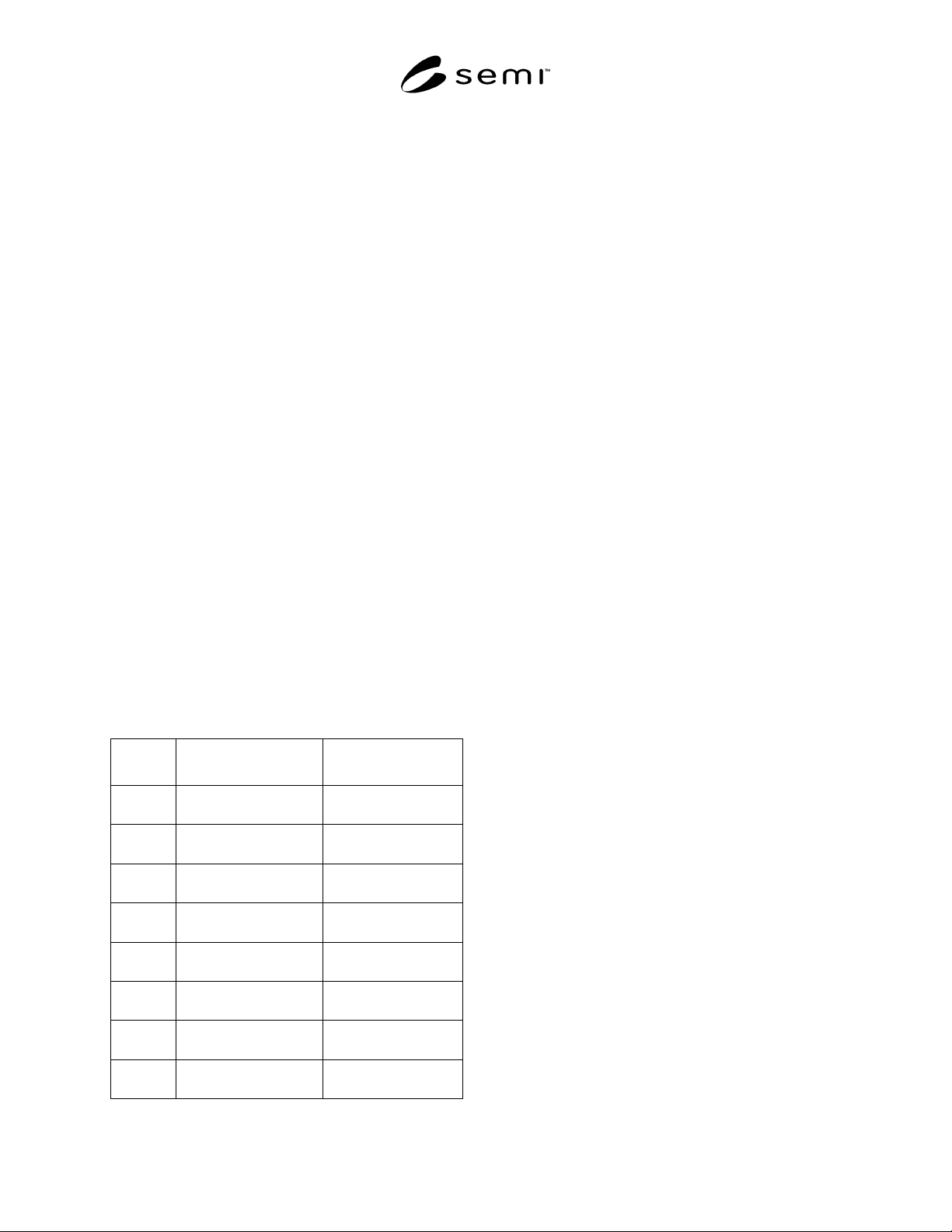
Table 1 Recommended Facility Electrostatic Levels
Year
Node
Electrostatic Discharge,
nC
Electrostatic Field,
V/cm V/inch
2000
180 nm
2.5–10 200 500
2002
130 nm
2.0 150 375
2003
100 nm
1.5 125 300
2004
90 nm
1.0 100 250
2007
65 nm
0.5 70 175
2009
50 nm
0.25 50 125
2012
32 nm
0.125 35 88
2015
25 nm
0.1 25 63
12.5.1 Since many decisions to use static control
materials will result in the permanent installation of
these materials, users may want to consider the eventual
use of their semiconductor facility in selecting the
acceptable electrostatic level. For example, at startup
the facility may be processing at 180-nm geometry, but
in five years it is anticipated to be at 90 nm. The
facility may need to be designed for the limits
recommended for the 90-nm use.
12.5.2 The levels in Table 1 assume that the
manufacturing facility is processing silicon
semiconductors. Manufacturers of specialized
components may need to choose lower levels.
Examples are manufacturers of gallium arsenide
semiconductors or magneto-resistive (MR) disk drive
read heads, those experiencing significant losses due to
contamination, or those using specialized equipment.
12.6 The levels listed in Table 1 have been determined
as the result of an analysis of working conditions, or
experiments done in operating semiconductor facilities.
Justifications for these levels are found in Appendix 1.
The actual levels to be used for any production area
may be decided by agreement between the user and
designer/builder of the facility.
12.7 Other levels may be appropriate under specific
operating conditions and for specific devices.
13 Calculations
13.1 A series of five measurements should be made.
The average of the five measurements should not
exceed the recommended level. No measurement
should exceed two times the recommended level.
14 Reporting Results
14.1 Data records should contain the following
information:
• Description of the materials or equipment under
test including model and serial numbers,
• Description of the factory operating conditions and
environment,
• Measurement equipment and last calibration date,
• Description of objects measured and measurement
locations,
• Humidity, temperature, and dew point at
measurement location when measurements were
made,
• Results of measurements,
• Personnel making the measurements, and
• Any other relevant comments.

SEMI E129-1103 © SEMI 2003 8
15 Test Method Precision and Accuracy
15.1 The test methods referenced in this document do
not guarantee precise measurements of static charge
levels. Similarly, maximum static charge levels
recommended in this document are not stated as precise
requirements. Accuracy of approximately ± 20% is
acceptable in all measuring instrumentation. At low
static charge levels, or for more accurate measurements,
alternative instrumentation and test methods may be
needed.
15.2 To evaluate low levels of electric field strength or
the voltage on an object, use an electrostatic fieldmeter
or electrostatic voltmeter with the resolution and
accuracy required. Under appropriate conditions,
electrostatic voltmeters exhibit a high degree of
accuracy and stability that is independent of the
distance from the charged object. The electrostatic
voltmeter probe can be located very close to a charged
surface without arc-over, and it is able to resolve the
field from a small charged object.
SEMI E129-1103 © SEMI 2003 9
APPENDIX 1
DEVELOPING THE RECOMMENDATIONS FOR ELECTROSTATIC
LEVELS
NOTICE: This appendix offers information related to the Electrostatic Levels contained in Section 12.5. It was
approved as an official part of SEMI E129 by full letter ballot procedures on September 3, 2003.
A1-1 Recommended Levels
A1-1.1 The recommended charge and electrostatic
field levels in this guide are not based on specific
protection thresholds for individual devices or process
tools. Rather, their aim is to classify the types of ESD
events or static levels that are likely to be of concern.
Facility designers and users should determine the types
of events that are of most concern to their products and
processes, to apply this guide to their needs.
Information on specific device damage thresholds is
best determined on an individual basis.
A1-2 Justification of Guide Recommendations
in Section 12.5 Table 1
A1-2.1 Recommendations for ESD Damage
A1-2.1.1 An analysis of the recommended levels to
protect semiconductor devices is found in Appendix 1
of SEMI E78. Related Information 1 of SEMI E78
discusses test methods for determining ESD damage
thresholds for semiconductor devices. Devices are
qualified according to the highest ESD stresses they can
withstand without measurable change in their operating
parameters. This section attempts to develop guide
recommendations for minimizing ESD damage based
on those discussions in SEMI E78.
A1-2.1.2 The information contained in SEMI E78 was
developed with respect to semiconductors handled by
equipment. It was current when published in 1998.
Device damage thresholds continue to decrease as
geometries get smaller, and although the classification
systems discussed in SEMI E78 have not changed,
more devices are falling into the more sensitive
classifications.
A1-2.1.3 It is desirable in this document to avoid
confusion with SEMI E78 sensitivity levels, as well as
to synchronize with the major changes in technology
mapped in the International Technology Roadmap for
Semiconductors (ITRS). Recommendations for
acceptable static charge levels are listed in Section 12.5
Table 1 and given for the major technology nodes of the
2003 ITRS, which relate to the size of the features on
the wafer.
A1-2.2 Charge Levels for ESD Damage
A1-2.2.1 Related Information 1.1 discusses test
methods for determining ESD damage thresholds for
semiconductor devices. Devices are qualified
according to the highest ESD stresses they can
withstand without measurable change in their operating
parameters. This section attempts to develop guide
recommendations for minimizing ESD damage based
on the discussion in Related Information 1.1.
A1-2.2.2 As discussed in Related Information 1.1.3,
ESD Simulator testing uses different capacitances for
each model. For Human Body Model (HBM) it is 100
pF, for Machine Model (MM) it is 200 pF, and for
Charged Device Model (CDM) it depends on the
capacitance of the actual device being tested. In any
case, it is charge (charge = voltage × capacitance) that
damages the device. It would seem appropriate,
therefore, that the guide recommendations in Table 1 in
Section 12.5 be stated in units of charge (e.g., nC).
A1-2.2.3 Based on industry testing reflected in device
data sheets, there appears to be a wide range for ESD
immunity in semiconductor devices, and it depends on
the type of ESD simulator used. HBM-type ESD
discharges are due to personnel handling and not likely
to occur within equipment. Charged equipment parts
contacting devices (i.e., MM) and charged devices
contacting machine parts (i.e., CDM) are the most
likely causes of ESD damage to devices in equipment.
A1-2.3 Industry Device Damage Levels
A1-2.3.1 The recommended electrostatic levels are
based on the following industry classifications. Each of
the test methods, (i.e., HBM, MM, and CDM) have a
set of qualification levels defined. These are contained
in Tables A1-1, A1-2, and A1-3 below.
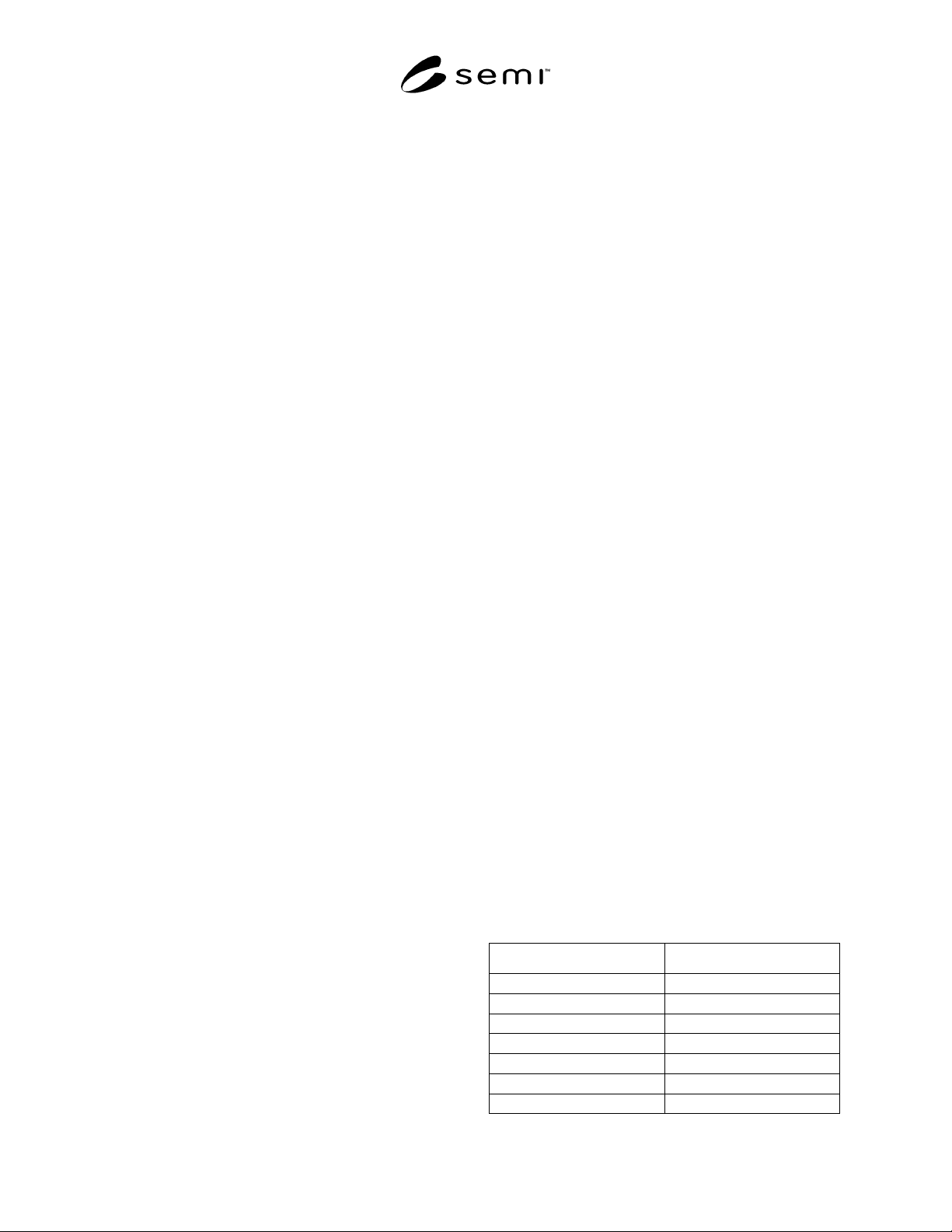
Table A1-1 HBM Classification Levels
Class Voltage, V
0 < 250
1A 250–499
1B 500–999
1C 1000–1999
2 2000–3999
3A 4000–7999
3B ≥ 8000