semi合集-English.pdf - 第4889页
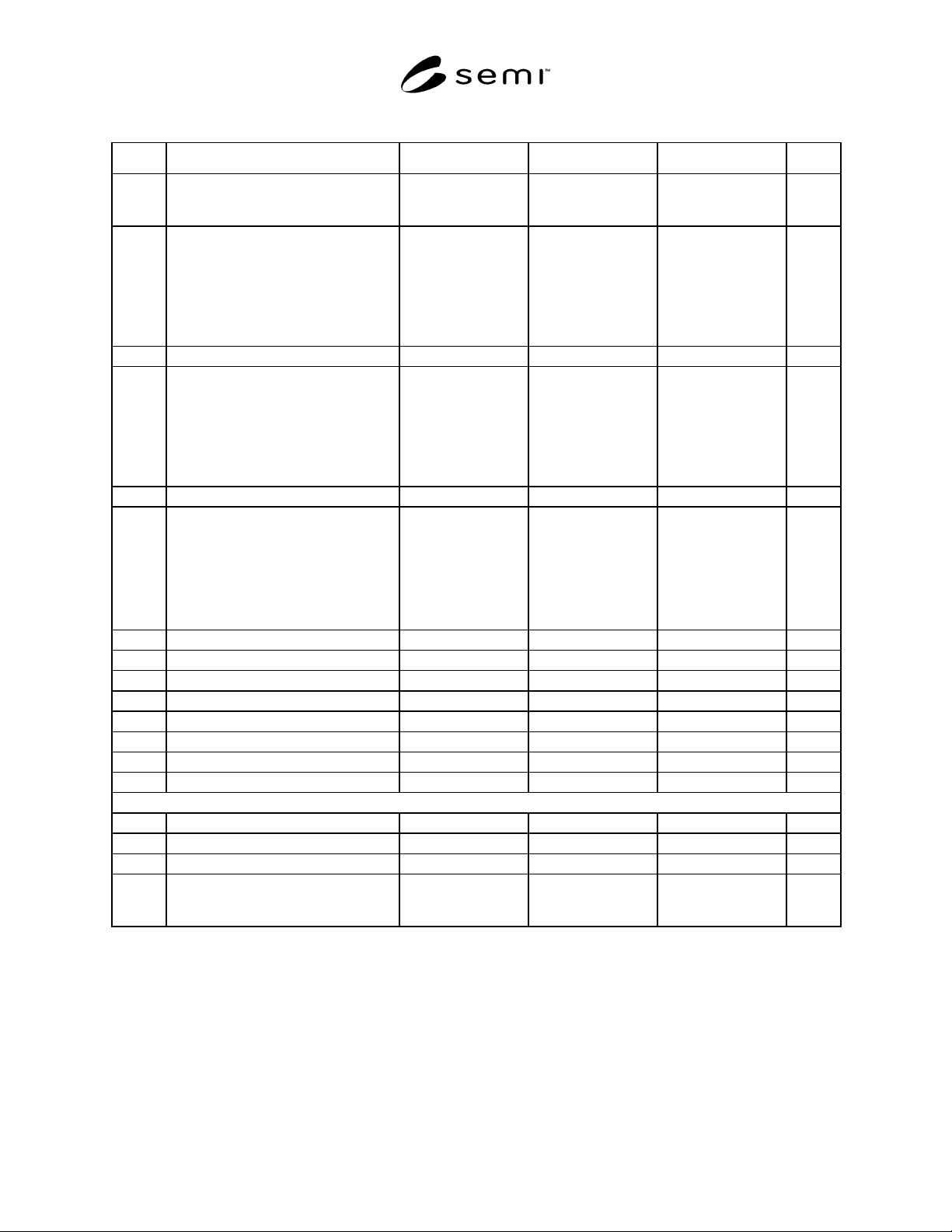
SEMI M3-0304 © SEMI 1978, 2004 9 Table R1-1 Recommende d Sapphire Substrate Defect Limits Item Characteristics Max Defect Limi t AQL (see NOTE 6) Illumination Notes 1 SCRATCHES Maximum Numbe r Maximum Length 3 R/2 High I…

SEMI M3-0304 © SEMI 1978, 2004 8
RELATED INFORMATION 1
RECOMMENDED SAPPHIRE SUBSTRATE FRONT SURFACE DEFECT
LIMITS
NOTICE: This related information is not an official part of SEMI M3 and was derived from the original edition of
the specifications which erroneously included this optional material as a part of the text of the specification. This
related information was approved for publication by full letter ballot procedure on September 3, 2003.
R1-1 Definitions for surface defects are found in SEMI MF523, where defects commonly found on silicon slices are
defined. Some of these terms do not apply to sapphire substrates, but are present in Table R-1, which lists
recommended limits for front surface defect levels, to provide a convenient reference point to the silicon wafer
standards, such as SEMI M1.
R1-1.1 Minimal Conditions and/or Dimensions — Minimal conditions or dimensions for defects are stated below
and shall be used for determining substrate acceptability unless other minimal limiters are agreed upon by the
interested parties. Anomalies less than these limits shall not be considered defects.
R1-1.2 Area Contamination — Foreign matter on the surface in localized areas which is revealed as discolored,
mottled, or cloudy appearance resulting from smudges, stains, water spots, etc.
R1-1.3 Contamination — Any foreign matter detectable under the inspection lighting conditions.
R1-1.4 Edge Chips and Indents — Any edge or surface anomaly conforming to the accepted definition greater than
0.010 inch in radial depth and peripheral length.
R1-1.5 Cracks — Any anomaly conforming to the accepted definition greater than 0.010 inch (0.25 mm) in total
length.
R1-1.6 Craters — Any individually distinguishable surface anomaly conforming to the accepted definition visible
when viewed under diffuse illumination.
R1-1.7 Crow’s Feet — N.A.
R1-1.8 Grooves — N.A.
R1-1.9 Haze — Haze is indicated when the image of a narrow beam tungsten lamp filament is detectable on the epi
silicon surface. (Under some conditions, contamination may appear as haze.)
R1-1.10 Mounds — N.A.
R1-1.11 Orange Peel — Any visually detectable roughened surface conforming to the accepted definition
observable under diffuse illumination.
R1-1.12 Pits — Any individually distinguishable nonremovable surface anomaly conforming to the accepted
definition visible when viewed under intense illumination.
R1-1.13 Saw Exit Mark — N.A.
R1-1.14 Scratch — Any anomaly conforming to the definition with a length-to-width ratio greater than 5:1.
R1-1.15 Striation — Any feature conforming to the accepted definition detectable under background lighting
conditions.
SEMI M3-0304 © SEMI 1978, 2004 9
Table R1-1 Recommended Sapphire Substrate Defect Limits
Item Characteristics Max Defect Limit AQL (see NOTE 6) Illumination Notes
1 SCRATCHES
Maximum Number
Maximum Length
3
R/2
High Intensity 1
2 PITS
Maximum Number
2" Diameter Substrate
3" Diameter Substrate
100 mm Diameter Substrate
125 mm Diameter Substrate
150 mm Diameter Substrate
4
9
15
20
25
4% Cum. 1, 2
3 HAZE None — see NOTE 4 4% Cum. 4
4 CONTAMINATION/PARTICULATE
Maximum Number
2" Diameter Substrate
3" Diameter Substrate
100 mm Diameter Substrate
125 mm Diameter Substrate
150 mm Diameter Substrate
4
9
15
20
25
4% Cum. Diffuse 1, 2
5 CONTAMINATION/AREA None
6 EDGE CHIPS
Maximum Number
Maximum Radial Penetration
Maximum Single Chip
Peripheral Length
Maximum Cumulative
Peripheral Length
see NOTE 3
2
0.12" (3 mm)
0.250" (6.35 mm)
0.250" (6.35 mm)
4% Cum. Diffuse 3
7 CRACKS, CROW' S FEET see NOTE 6 6
8 CRATERS None 1, 5
9 DIMPLES None 1
10 GROOVES None 4% Cum. 1, 5
11 MOUNDS None 1, 5
12 ORANGE PEEL None Diffuse 1
13 SAW MARKS None 1, 5
14 STRIATIONS
SLICE BACK SURFACE
15 CHIPS see NOTE 3 see NOTE 3 Diffuse 3
16 CRACKS, CROW' S FEET None see Note 6 6
17 CONTAMINATION/AREA None
18 SAW MARKS
Incidence
Maximum Depth
N.A. see Note 5 5
NOTE 1: The outer 4 mm annulus is excluded from these criteria.
NOTE 2: Ninety percent of substrate shall be free of contaminants after pre-inspection treatment. Balance of substrate may have light-reflecting
particles up to the limit established for Item 2 — Pits.
NOTE 3: All chips shall be beveled. Chips less than 0.4 mm should not be counted.
NOTE 4: Haze refers to epitaxial silicon appearance only, not to condition of polished sapphire substrate.
NOTE 5: These defects are not observed in SOS wafers. Terms remain for convenient reference to silicon specification.
NOTE 6: Cracks are observed in sapphire substrates as fractures or as surface separations along cleavage planes. The cumulative AQL for both
front surface and back surface of substrate is 4% for both. Crow’s feet see Note 5.
SEMI M3-0304 © SEMI 1978, 2004 10
RELATED INFORMATION 2
RECOMMENDED SURFACE FINISH CHARACTERISTICS FOR
SAPPHIRE SUBSTRATES
NOTICE: This related information is not an official part of SEMI M3 and was derived from the original edition of
the specifications which erroneously included this optional material as a part of the text of the specification. This
related information was approved for publication by full letter ballot procedure on September 3, 2003.
R2-1 Front Surface Finish
R2-1.1 The substrate should be polished on one side suitable for the epitaxial growth of silicon.
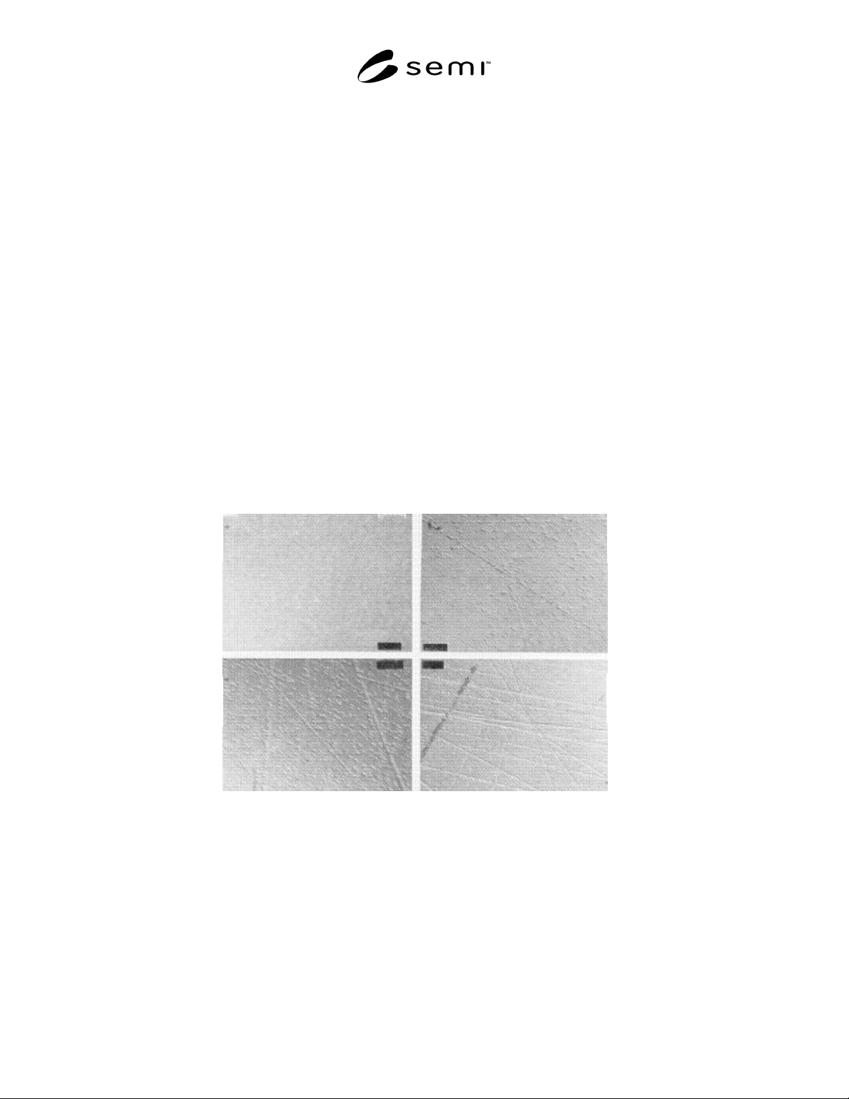
R2-1.2 The quality of this surface may be determined by optical examination at 70× using Nomarski interference
contrast microscopy after etching the substrate in potassium hydroxide at 310°C for one to three minutes.
R2-1.3 The photomicrographs in Figures R2-1 through R2-4 may be used as a surface quality guide.
R2-1.3.1 Figure R2-1 shows an acceptable surface.
R2-1.3.2 Figures R2-2 and R2-3 show questionable surfaces that are subject to individual evaluation.
R2-1.3.3 Figure R2-4 shows an unacceptable surface.
R2-2 Back Surface Finish
R2-2.1 The recommended back surface finish is approximately 32 µin, rms, as determined by stylus or optical
profilometer.
Figure R2-1
Acceptable
Surface
Figure R2-3
Questionable
Surface
Figure R2-2
Questionable
Surface
Figure R2-4
Unacceptable
Surface
Figures R2-1 through R2-4
Illustrations of Acceptable, Unacceptable, and Questionable Sapphire Substrate Front Surface Finishes.
NOTICE: SEMI makes no warranties or representations as to the suitability of the standards set forth herein for any
particular application. The determination of the suitability of the standard is solely the responsibility of the user.
Users are cautioned to refer to manufacturer’s instructions, product labels, product data sheets, and other relevant
literature respecting any materials mentioned herein. These standards are subject to change without notice.
The user’s attention is called to the possibility that compliance with this standard may require use of copyrighted
material or of an invention covered by patent rights. By publication of this standard, SEMI takes no position
respecting the validity of any patent rights or copyrights asserted in connection with any item mentioned in this
standard. Users of this standard are expressly advised that determination of any such patent rights or copyrights, and
the risk of infringement of such rights, are entirely their own responsibility.
Copyright by SEMI® (Semiconductor Equipment and Materials
International), 3081 Zanker Road, San Jose, CA 95134. Reproduction o
f
the contents in whole or in part is forbidden without express written
consent of SEMI.