semi合集-English.pdf - 第5939页
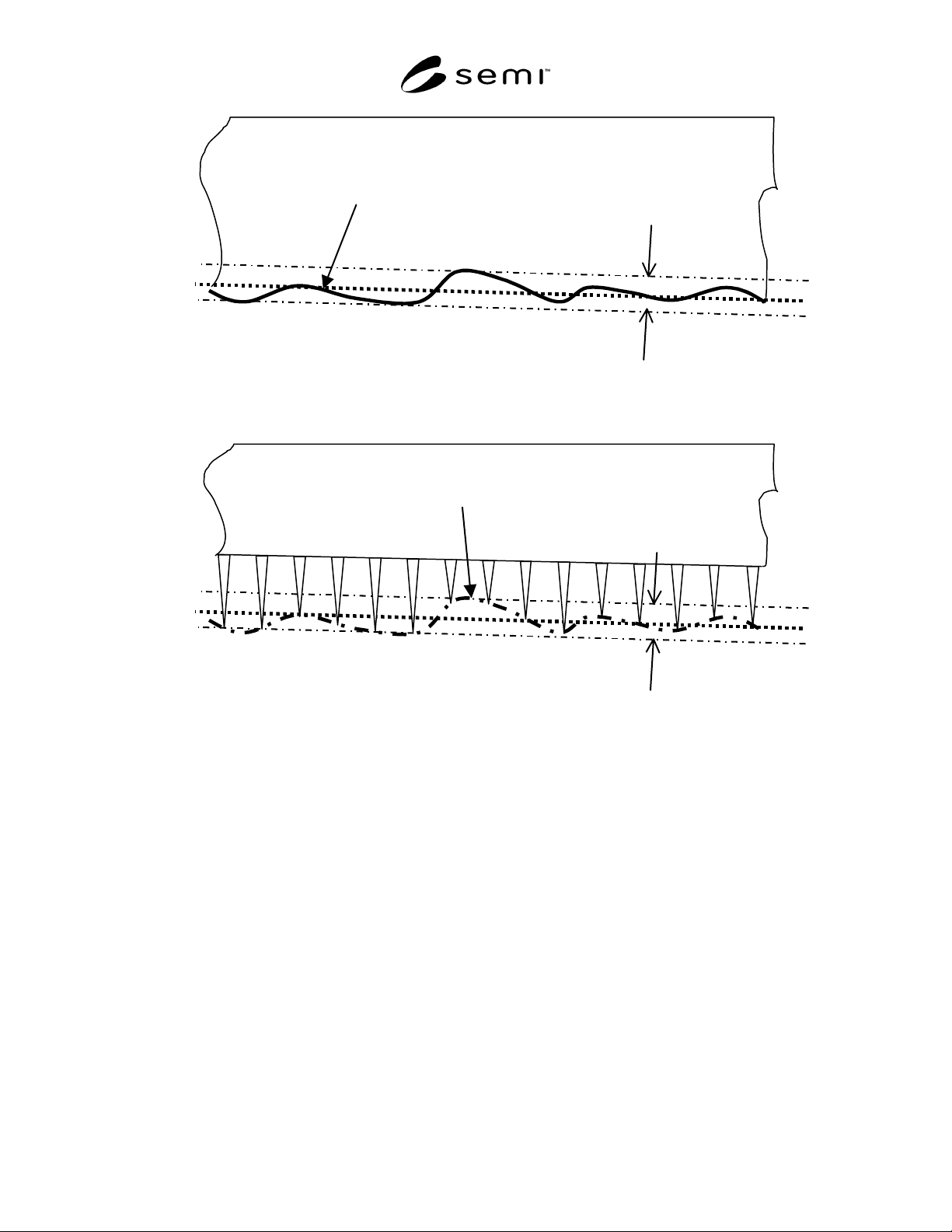
SEMI P40-1103 © SEMI 2003 5 P 1 Mounting surf ace Flatnes s error Chuck Figure 3 Definition of Flatness Error P 1 is the best fit plane that minimiz es th e maximum deviation of the surface from P 1 . P 1 Mounting surf a…
SEMI P40-1103 © SEMI 2003 4
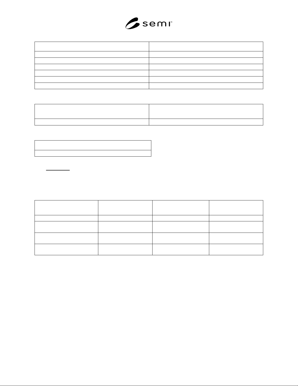
Table 1 Flatness of the Mounting Surface
Any Square Region with Specified Edge Length (millimeters) Peak-to-Valley Flatness (nanometers)
150 48
75 24
40 12
25 8
20 6
10 3
Table 2 Clamping Pressure
Mean Clamping Pressure (KPa) Maximum Range of Clamping Pressure within Flatness Quality
Area (KPa)
15 ± 1.5
3.0
Table 3 Minimum Effective Bending Stiffness of the Chuck Cross Section
Bending Stiffness (Newton-meter) (See Note 1.)
30,000
NOTE 1: The effective bending stiffness (D) of a chuck with a solid cross section is given by:
D =
Eh
3
12 1 −
ν
2
()
where E is the elastic modulus in N/m
3
, h is the thickness in meters and ν is Poisson’s ratio.
Table 4 Dimensions of Pins or Pedestals on Chuck Surface
Parameter Label for parameter in
Figure 5
Units Required Value
Maximum spacing S
p
millimeters 10
Period P
p
millimeters To be agreed upon between
user and supplier
Angle of sidewall
θ
degrees To be agreed upon between
user and supplier
Pin height H
p
microns To be agreed upon between
user and supplier
SEMI P40-1103 © SEMI 2003 5
P
1
Mounting surface
Flatness error
Chuck
Figure 3
Definition of Flatness Error
P
1
is the best fit plane that minimizes the maximum deviation of the surface from P
1
.
P
1
Mounting surface
Flatness error
Chuck
Figure 4
Definition of Flatness Error for a Pin or Pedestal Chuck
P
1
is the best fit plane that minimizes the maximum deviation from the surface that passes through the
highest points on the chuck surface.
SEMI P40-1103 © SEMI 2003 6
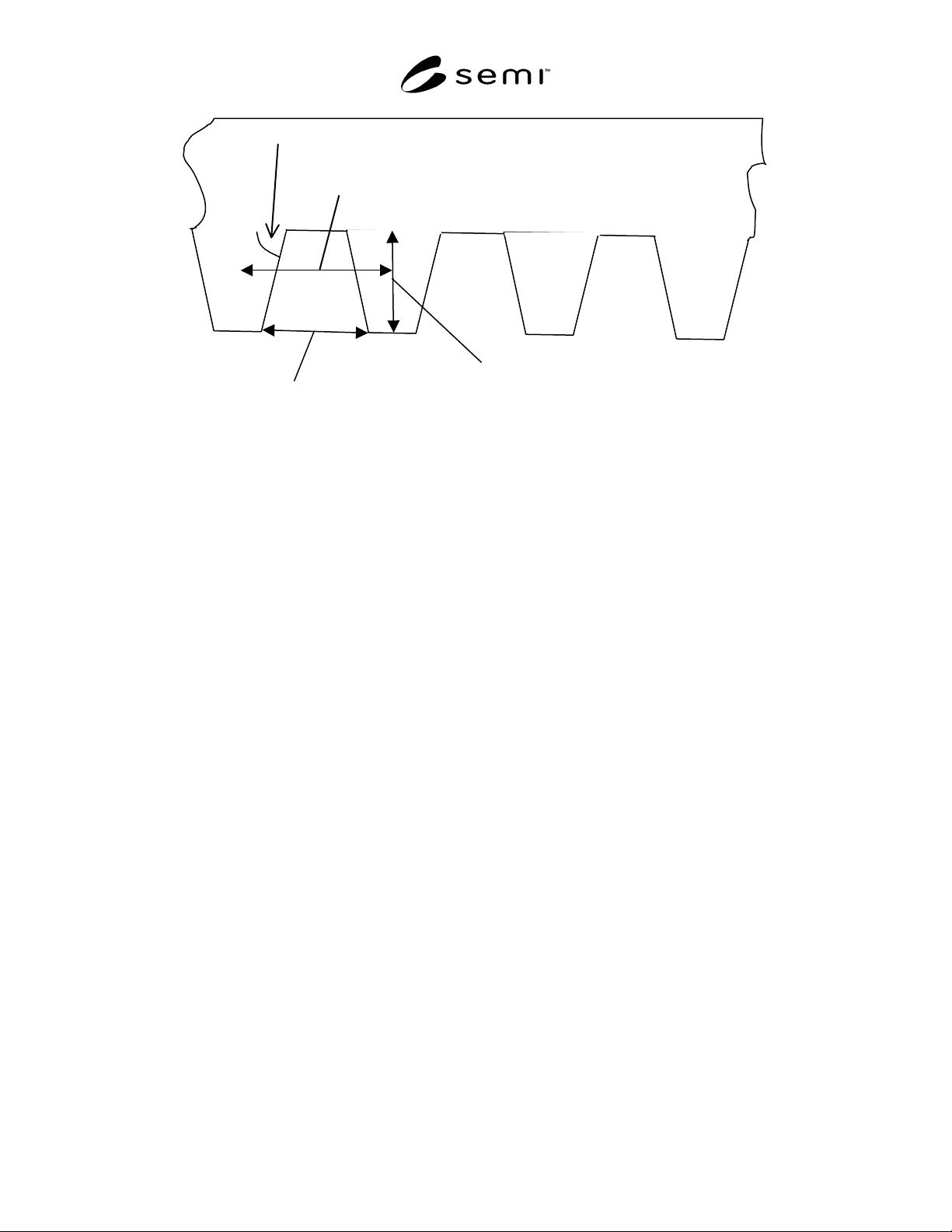
Pin sidewall angle
Chuck
Pin spacing, S
p
θ
Pin period, P
p
Pin height, H
p
Figure 5
Dimensions of Pins or Pedestals on the Chuck Surface
NOTICE: SEMI makes no warranties or representations as to the suitability of the standards set forth herein for any
particular application. The determination of the suitability of the standard is solely the responsibility of the user.
Users are cautioned to refer to manufacturer' s instructions, product labels, product data sheets, and other relevant
literature, respecting any materials or equipment mentioned herein. These standards are subject to change without
notice.
By publication of this standard, Semiconductor Equipment and Materials International (SEMI) takes no position
respecting the validity of any patent rights or copyrights asserted in connection with any items mentioned in this
standard. Users of this standard are expressly advised that determination of any such patent rights or copyrights, and
the risk of infringement of such rights are entirely their own responsibility.
Copyright by SEMI® (Semiconductor Equipment and Materials
International), 3081 Zanker Road, San Jose, CA 95134. Reproduction o
f
the contents in whole or in part is forbidden without express written
consent of SEMI.