semi合集-English.pdf - 第5229页
SEMI M40-0200 © SE MI 2000 11 A P PENDIX 1 NOT E: The mate rial in this appe ndix is an of ficial pa rt of SEMI M40 an d was approv ed by full le tter ballo t procedures on December 15 , 1999 b y the North American Regio…
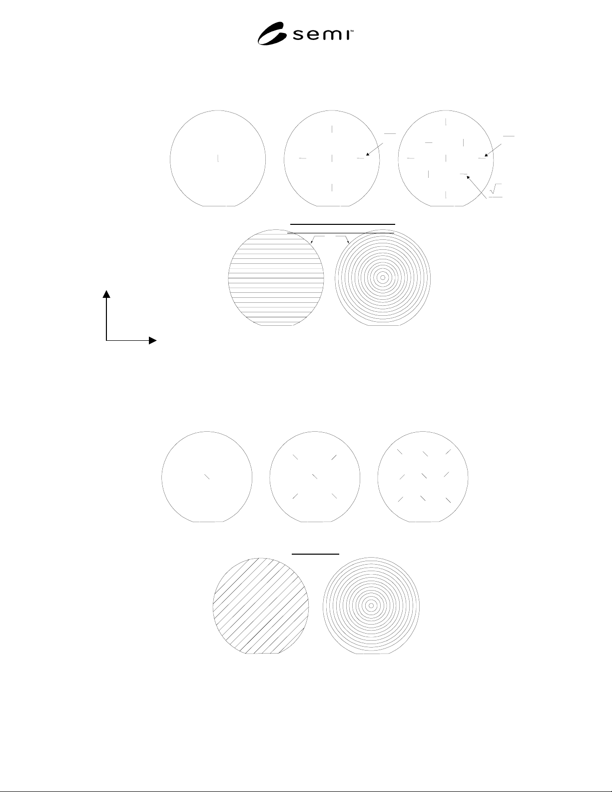
SEMI M40-0200 © SEMI 2000 10
Center Point *
Raster Scan
R-Theta
Five Point *
Nine Point *
11
7
8
9
6
4
4
2
2
333
5
5
Type A Local Scan Patterns
*
* Line indicates scan direction for all line scans.
Centerpoint of line = location for point measurements
**
** Scan patterns to full FQA
2
3
r
4
5
r
2
5
r
Full FQA Scan Patterns
X
Y
Wafer and Scan
Coordinate System
Center Point
Five Point Nine Point
1
1
7
8
9
6
4
4
2
2
3
3
5
5
Raster Scan
R-Theta
Full FQA
Type B Local Scan Patterns
Figure 1
Patterns of Locations on a Silicon Wafer Surface for Measuring
(NOTE: R-Theta scan may be implemented in either a circular or a spiral pattern.)

SEMI M40-0200 © SEMI 200011
APPENDIX 1
NOTE: The material in this appendix is an official part of SEMI M40 and was approved by full letter ballot procedures on
December 15, 1999 by the North American Regional Standards Committee.
A1-1 Examples of Roughness Measurement Specifications and Related Output
The construction of typical measurement specifications and reported results are shown below. These could be the
input to and output from a suitably equipped metrology tool, or directions for manual execution and reporting of the
measurement and calculation sequence. The elements and codes are listed only in the first example. The
quantitative data below is presented for illustration only, it does not represent actual instrument or sample
measurements.
1. Mechanical Profiler
The Mechanical profiler measurement was specified as MPR,5,L,A,A,A,250/10. This corresponds to
measuring a 5-point pattern with a local line-scan and with pattern orientation A, and reporting Ra average
value over a bandwidth from 250 to 10 µm.
Elements Profiler, Mechanical; 5-point; line-scan; orient A; Ra; average; 250/10 µm
Codes MPR 5 L A A A 250/10
Output Example MPR,5,L,A,A,A,250/10 = 0.53 nm
2. Angle-Resolved Light Scattering
The Angle-resolved light scattering instrument measurement was specified as ARLS,9,B,P,Q,A,40/2.0. This
corresponds to measuring a 9-point pattern with a single spot and with pattern orientation B, reporting rms (Rq)
average value over a bandwidth from 40 to 2 µm.
Output Example ARLS,9,B,P,Q,A,40/2.0 = 0.15 nm
3. Interference Microscope
The Interference microscope measurement was specified as IM,5,A,A,T,D,250/10. This corresponds to
measuring a 5-point pattern with a local area and with pattern orientation A, reporting peak-to-valley (Rt)
standard deviation over a bandwidth from 250 to 10 µm.
Output Example IM,5,A,A,T,D,250/10 = 0.05 nm
4. Total Integrated Scattering
The Total Integrated Scattering system (TIS) measurement was specified as TIS,S,P,A,Q,D,38/0.50. This
corresponds to measuring a full FQA/spiral scan with a local spot and with pattern orientation A, reporting rms
(Rq) standard deviation over a bandwidth from 38 to 0.5 µm.
Output Example TIS,S,P,A,Q,D,38/0.50 = 0.02 nm
5. Optical Profiler
The Optical Profiler measurement was specified as OPR,9,L,B,A,AD,80/0.50. This corresponds to measuring a
9 point pattern with a local line-scan and with pattern orientation B, reporting Ra average value and standard
deviation over a bandwidth from 80 to 0.5 µm.
Output Example OPR,9,L,B,A,AD,80/0.50 = 0.17nm (Ra average), 0.02 nm (Ra, standard
deviation)
6. AFM
The AFM measurement was specified as AFM,5,A,A,Z,A,20/0.04. This corresponds to measuring a 5 point
pattern with local area and with pattern orientation A, reporting Rz average value over a bandwidth from 20 to
0.040 µm.
Output Example AFM,5,A,A,Z,A,20/0.04 = 0.43 nm

SEMI M40-0200 © SEMI 2000 12
NOTICE: SEMI makes no warranties or representations as to the suitability of the guide set forth herein for any
particular application. The determination of the suitability of the guide is solely the responsibility of the user. Users
are cautioned to refer to manufacturer’s instructions, product labels, product data sheets, and other relevant literature
respecting any materials mentioned herein. These guides are subject to change without notice.
The user’s attention is called to the possibility that compliance with this guide may require use of copyrighted
material or of an invention covered by patent rights. By publication of this guide, SEMI takes no position respecting
the validity of any patent rights or copyrights asserted in connection with any item mentioned in this guide. Users of
this guide are expressly advised that determination of any such patent rights or copyrights, and the risk of
infringement of such rights, are entirely their own responsibility.