semi合集-English.pdf - 第5892页
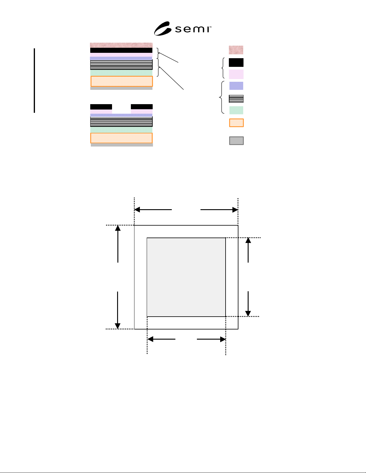
SEMI P38-1103 © SEMI 2002, 2003 4 Substrate A bsorber layer(s) Buffer lay er Mu l t i l a y e r Capping lay er(s) Patterned mask Unpatterned mask or mask blank Abs o rb er stack Mult ilay er stack Underlay er(s) Resi st …

SEMI P38-1103 © SEMI 2002, 2003 3
10 Sampling
10.1 Unless otherwise specified, appropriate sample
sizes shall be selected from each lot in accordance with
ANSI/ASQC Z1.4. Each quality characteristic shall be
assigned an acceptable quality level (AQL) in
accordance with ANSI/ASQC Z1.4 definitions for
critical, major, and minor classifications. If desired, and
so specified in the contract or order, each of these
classifications may alternatively be assigned cumulative
AQL values. The method of certification shall be
agreed upon between user and supplier.
11 Test Methods
11.1 Thickness Method of measuring layer
thickness values to be agreed upon between user and
supplier.
11.2 Reflectivity Method of measuring reflectivity at
specified wavelengths to be agreed upon between user
and supplier with these exceptions:
11.2.1 Each individual reflectivity measurement should
represent reflectivity over an area having rectangular
dimensions < 1 mm.
11.2.2 EUV reflectivity must be measured at 6 degrees
with respect to the normal to the plane of the mask
blank surface.
11.3 Stress Method of measuring stress is to be
agreed upon between user and supplier.
11.4 Outgassing Method of measuring outgassing
rate is to be agreed upon between user and supplier.
11.5 Etch Rates Method of measuring etch rates and
etch selectivity is to be agreed upon between user and
supplier.
11.6 Defects Method of inspection for defects is to
be agreed upon between user and supplier.
11.7 Flatness Method of measuring flatness is to be
agreed upon between user and supplier.
11.8 Backside Sheet Resistance Method of
measuring sheet resistance is to be agreed upon
between user and supplier.
11.9 Electrical Resistance method of measuring
electrical resistance is to be agreed upon between user
and supplier.
12 Certification
12.1 Upon request of the purchaser in the contract or
order, a manufacturer’s or supplier’s certification that
the material was manufactured and tested shall be
provided in accordance with this specification.
13 Packing and Labeling
13.1 Mask blanks shall be packed in a Class 1
environment. Containers shall be designed to prevent
blank-to-blank contact and to protect the substrates
from contamination in handling and transit. Substrates
shall be shipped with the coated side facing toward the
same end of the box. This orientation shall be indicated
on each container. Packaging shall comply with the
applicable international, national, state laws, and local
regulations required for shipping.
13.2 Containers shall be labeled, “Warning: Open and
Handle Under Clean Room Conditions Only.” Each
shipment shall be identified by user purchase order
number, drawing number (if applicable), quantity,
supplier lot number, and material identification.
Material identification methodology to be agreed upon
between user and supplier.
13.3 Each mask blank shall be labeled with an
alphanumeric sequence that contains the items listed in
Table 15 in sequential order. No spaces will be
included, and each item listed in Table 15 shall be
separated by a dash in the text of the label. Note that
the class values for different properties of a mask blank
are determined individually.
SEMI P38-1103 © SEMI 2002, 2003 4
Substrate
Absorber layer(s)
Buffer layer
Multilayer
Capping layer(s)
Patterned mask
Unpatterned mask or mask blank
Absorber
stack
Multilayer
stack
Underlayer(s)
Resist
Conductive layer
Multilayers
Figure 1
Definition of Absorber, Buffer, Capping Layer, Multilayers, Absorber Stack, and Multilayer Stack
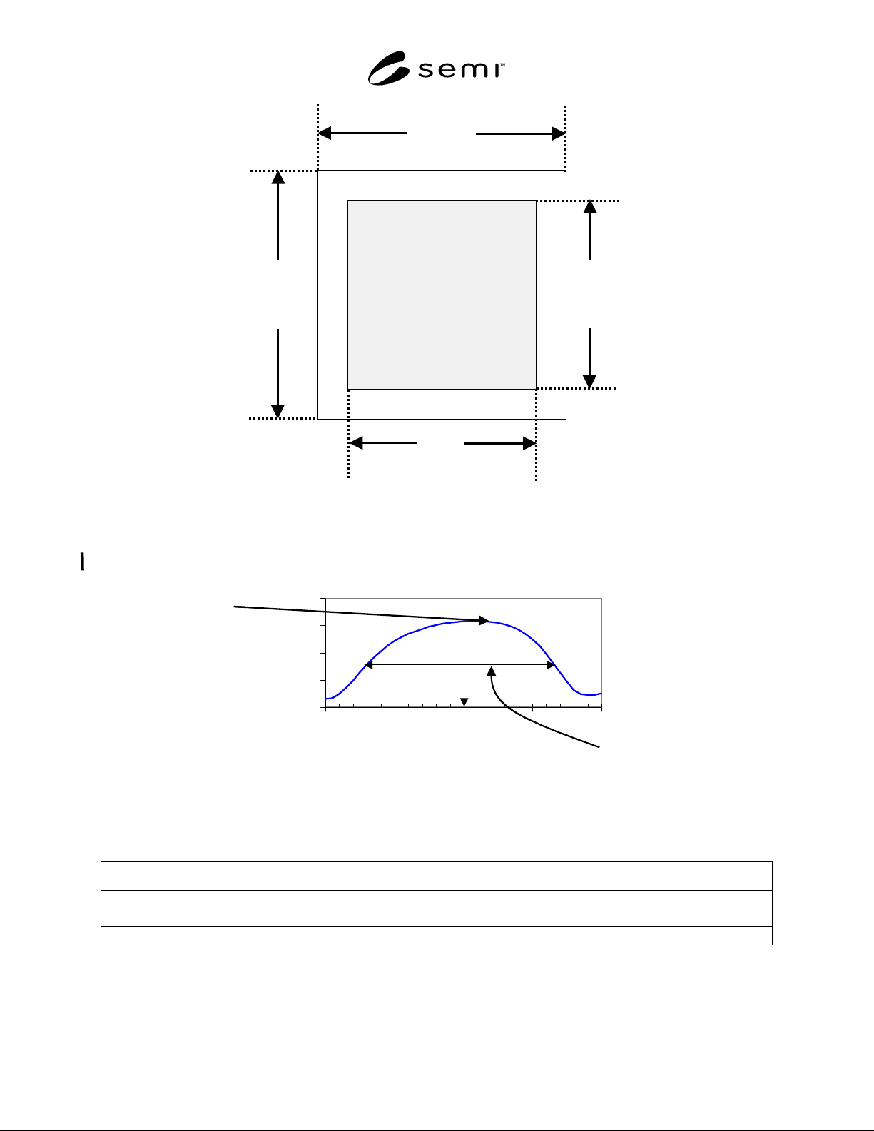
D
l
W
l
Layer
quality
area
L
L
D
L
W
L
Figure 2
Dimensions of Layer Quality Area
SEMI P38-1103 © SEMI 2002, 2003 5
L
D
d
W
d
Defect
quality
area
L
Figure 3
Dimensions of Defect Quality Area
0%
20%
40%
60%
80%
13 13.2 13.4 13.6 13.8
Wavelength (nm)
Reflectivity
Median wavelength of mask = (λ
2
+ λ
1
)/2
Full width at half
maximum (FWHM)
Peak reflectivity
λ
2
λ
1
0%
20%
40%
60%
80%
13 13.2 13.4 13.6 13.8
Wavelength (nm)
Reflectivity
Median wavelength of mask = (λ
2
+ λ
1
)/2
Full width at half
maximum (FWHM)
Peak reflectivity
λ
2
λ
1
Median wavelength of EUV reflectivity of mask = (λ
2
+ λ
1
)/2
Figure 4
EUV Reflectivity of Multilayer Stack
Table 1 Mask Blank Type
Type Layers or groups of layers included in addition to the substrate
1 Conductive layer and multilayer stack
2 Conductive layer, multilayer stack, and absorber stack
3 Conductive layer, multilayer stack, absorber stack and resist