semi合集-English.pdf - 第7213页
SEMI MF26-0305 © SEMI 2003, 2005 3 2 2 2 l k h a d (2) 4.1.1.2 The angle, , may then be found from the following modified form of Bragg’s law for cubic lattice structures: a l k h n 2 sin 2 2 2 (3) 4.1.…
SEMI MF26-0305 © SEMI 2003, 2005 2
E 177 — Practice for Use of the Terms Precision and Bias in ASTM Test Methods
3
3.3 ANSI Standard
B74.10 — Specifications for Grading of Abrasive Microgrits
4
3.4 Other Standard
Code of Federal Regulations, Title 10, Part 20, Standards for Protection Against Radiation
5
NOTICE: Unless otherwise indicated, all documents cited shall be the latest published versions.
4 Test Method A — X-Ray Diffraction Orientation
4.1 Summary of Test Method
4.1.1 The atoms of a single crystal form a periodic three-dimensional array in a crystal lattice structure whose units
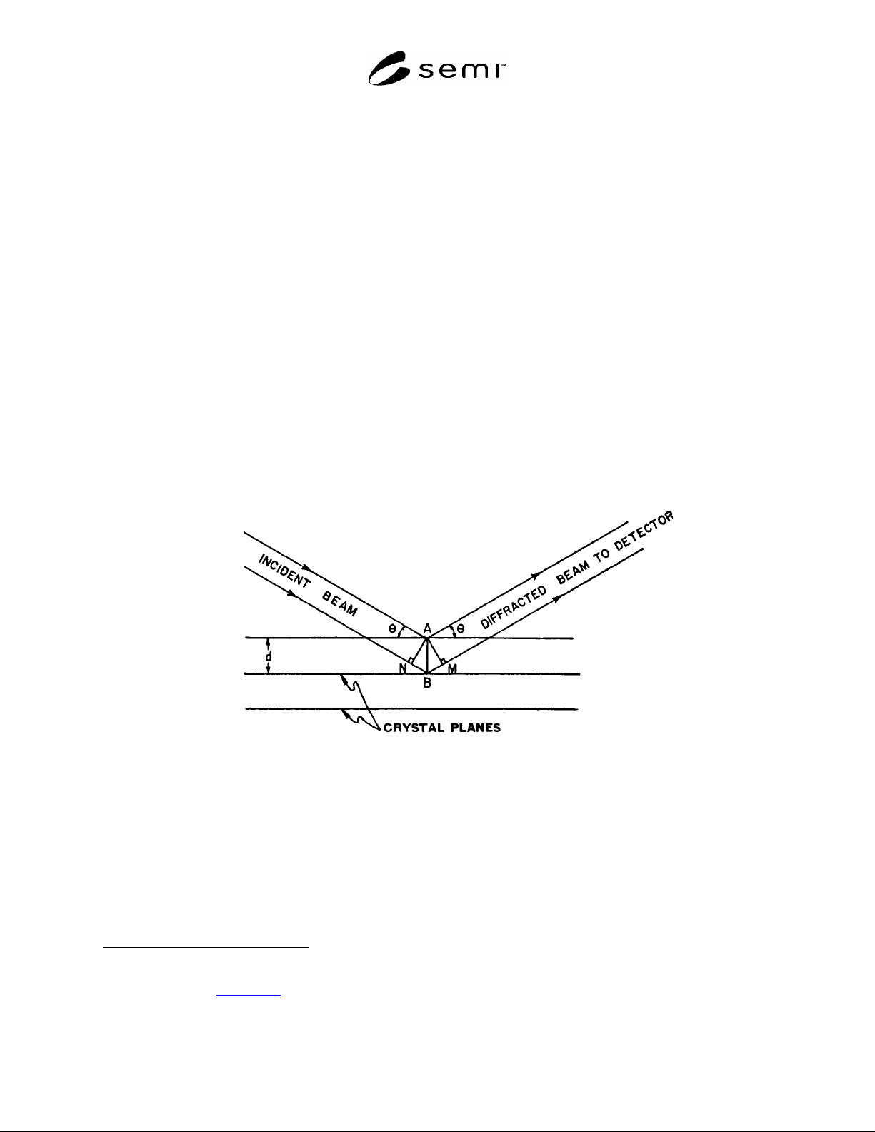
may be considered as lying in a series of parallel planes of equal perpendicular spacing, d, as shown in Figure 1.
When a beam of parallel, monochromatic X rays of wavelength
is incident upon the planes, diffraction (reflection)
occurs when the path difference of the X rays between adjacent planes is an integral number, n, of wavelengths.
When this geometrical condition is satisfied, the reflections from the various planes of the series are exactly in phase
and the diffracted beam is of maximum intensity. Thus, as shown in Figure 1, the diffracted beam of X rays
possesses maximum intensity when the angle of incidence,
, of the beam with the reflecting planes, the X-ray
wave-length,
, the atomic interplanar spacing, d, and the order of the diffraction, n, simultaneously have values that
obey Bragg’s law as follows:
sin2dn
(1)
NOTE: Reflection conditions are as follows: NB = BM = dsin
, NB + BM = n
, n
= 2dsin
.
Figure 1
Geometrical Reflection Conditions for X Rays from a Single Crystal
4.1.1.1 The reflecting planes are more commonly defined in terms of their Miller indexes (h, k, l). The Miller
indexes are the smallest integers proportional to the reciprocals of the intercepts of the plane on the three crystal
axes of unit length. Thus, for any lattice structure where the periodicity is represented by a cubic unit cell of side
length (lattice parameter), a, the lattice spacing, d, of a set of parallel atomic planes, may be written as follows:
3 Annual Book of ASTM Standards, Vol 14.02.
4 American National Standards Institute, New York Office: 25 West 43rd Street, New York, NY 10036, USA. Telephone: 212-642-4900; Fax:
212-398-0023, Website:
www.ansi.org
.
5 Published in Federal Register, Nov. 17, 1960. Available from Superintendent of Documents, U.S. Government Printing Office, Washington,
DC 20402.
SEMI MF26-0305 © SEMI 2003, 2005 3
222
lkh
a
d
(2)
4.1.1.2 The angle,
, may then be found from the following modified form of Bragg’s law for cubic lattice
structures:
a
lkhn
2
sin
222
(3)
4.1.1.3 In the diamond cubic structure, to which silicon and germanium, the Group IV semiconductors, belong, and
in the zinc blende structure, to which gallium arsenide and the other Group III–Group V semiconductors belong, the
following general rule gives the commonly observed reflections: h, k, and l must be all even or all odd, with the
further restriction that when h, k, and l are all even, then h + k + l must be divisible by four. Values of
for various
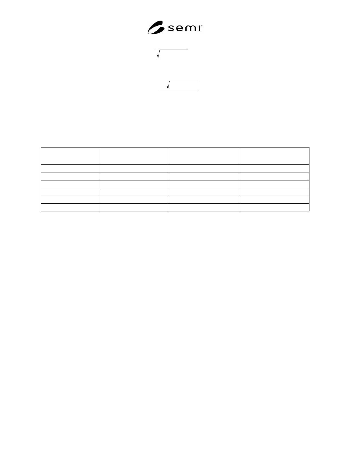
low-order reflections, h, k, l, are given in Table 1 for silicon, germanium, and gallium arsenide.
Table 1 Bragg Angles,
, for X-ray Diffraction of CuK
Radiation in Semiconductive Crystals (
= 1.54178 Å)
Reflecting Planes h, k, l
Silicon
a = 5.43073 Å (±0.00002 Å)
#1, #2
Germanium
a = 5.6575 Å (±0.00001 Å)
#1, #3
Gallium Arsenide
a = 5.6534 Å (±0.00002 Å)
#1, #4
111
14°14 13°39 13°40
220
23°40 22°40 22°41
311
28°05 26°52 26°53
400
34°36 33°02 33°03
331
38°13 36°26 36°28
422
44°04 41°52 41°55
#1 a = lattice parameter value.
#2 Bond, W. L., and Kaiser, W., J. Phys. Chem. Solids 16, 44 (1960).
#3 Greiner, E. S., J. Metals 4, 1044 (1952).
#4 Giesecke, G., and Pfister, H., Acta Crystallographica 11, 369 (1958).
4.1.2 The orientation of a single crystal surface is the crystallographic plane, described in terms of its Miller
indices, with which the surface is ideally coincident. In semiconductive single crystals, where the cross-sectional
plane of the crystal or the surface of a wafer cut from the crystal usually corresponds within several degrees to a low
index crystallographic plane, such as a (100) or (111) plane, the orientation is frequently described in terms of the
maximum angular deviation of the low index crystallographic plane from the mechanically prepared surface. Other
crystallographic planes may be found with respect to this low index plane by using a table of angles between
crystallographic planes of a cubic crystal. Such a table appears in ASTM Test Method E 82.
4.1.3
The angular deviation of a reflecting plane from a prepared reference surface is found by determining two
components of the deviation in two planes perpendicular to each other and to the reference surface. Each of the
deviation components represents a setting of the crystal lattice that satisfies Bragg's law for the particular X-ray
beam configuration. The reference surface itself must be perpendicular to the plane of the incident and reflected
beams. Initially, an orientation determination is made at any arbitrary position of the crystal. Then the crystal is
rotated 90° of arc about the normal to the reference surface (the normal lying in the plane of the incident and
reflected beams) and a second orientation determination made. The crystal is rotated another 90° of arc (in the same
direction) and a third orientation determination is made. The crystal has now been rotated 180° of arc with respect
to the starting point. The crystal is then rotated another 90° of arc (that is, 270° of arc from the starting point) and a
fourth orientation determination is made.
4.1.4
These four measurements are combined to determine both the instrument error and the two components of the
angular deviation,
and
, between the reference surface under investigation and the desired crystallographic plane.
This information facilitates slicing of the crystal along the desired plane or alternatively the determination of the
maximum angular deviation.

SEMI MF26-0305 © SEMI 2003, 2005 4
4.2 Apparatus
4.2.1 X-Ray Apparatus, commercially available, utilizing a copper-target tube, gives satisfactory results. The X-ray
beam is collimated by means of a slit system to give parallel rays, and the X rays are passed through a thin nickel
filter to give a beam that is essentially monochromatic. The specimen is placed in a holder so that the surface under
investigation contains the axis about which the specimen is rotated in satisfying the Bragg law conditions. Rotations
about this axis are measured on a scale in degrees and minutes of arc. The holder must also permit rotation of the
specimen about a normal to the surface under investigation. The Bragg angle corresponding to the particular X-ray
wavelength used, the material under investigation, and the particular family of planes being oriented must be known
from Table 1 or be determined. A suitable detector, such as a Geiger counter, is positioned so that the angle
between the extension of the incident X-ray beam and the line joining the counter and the axis of rotation of the
specimen is twice the Bragg angle. It is essential that the incident X-ray beam, the diffracted beam, the reference
surface normal, and the detector opening all lie in the same plane.
4.3
Hazards
4.3.1 Too much emphasis cannot be placed on the necessity of avoiding personal exposure to X rays. It is
especially important to keep hands or fingers out of the path of the X rays and to protect the eyes from scattered
secondary radiation. The use of commercial film badge or dosimeter service is recommended together with periodic
checks of the radiation level at the hand and body positions with a Geiger-Müller counter calibrated with a standard
nuclear source. The present maximum permissible dose for total body exposure of an individual to external X
radiation of quantum energy less than 3 MeV over an indefinite period is 1.25 R (3.22 × 10
4
C/kg)/calendar quarter
(equivalent to 0.6 mR/h (1.5 × 10
7
C/kg·h)) as established in the Code of Federal Regulations, Title 10, Part 20.
The present maximum permissible dose for hand and forearm exposure under the same conditions is 18.75 R
(4.84 × 10
3
C/kg)/calendar quarter (equivalent to 9.3 mR/h (2.4 × 10
6
C/kg·h)).
4.4 Procedure
4.4.1 Adjust the surface under investigation about the axis of rotation perpendicular to the incident and reflected
beams until the diffracted intensity is at a maximum.
4.4.2 Record, to the nearest minute, as
1
, the angle indicated on the scale.
4.4.3 Rotate the specimen through 90° of arc about a normal to the (reference) surface under investigation. Repeat
the procedure of ¶4.4.1 and record, to the nearest minute, as
2
, the angle indicated on the scale.
4.4.4 Rotate the specimen another 90° of arc in the same direction (that is, 180° from the original position). Repeat
the procedure of ¶4.4.1 and record, to the nearest minute, as
3
, the angle indicated on the scale.
4.4.5 Rotate the specimen another 90° of arc in the same direction (that is, 270° of arc from the original position).
Repeat the procedure of ¶4.4.1 and record, to the nearest minute, as
4
, the angle indicated on the scale.
4.5 Calculations
4.5.1 Calculate and record the angular deviation components,
and
, as follows:
)(
2
1
31
(4)
and
)(
2
1
42
(5)
4.5.2 Calculate and record the total angular deviation,
, between the surface under consideration and the desired
crystallographic plane as follows:
coscoscos
(6)
where
and
are the two components of the total angular deviation,
. For angles smaller than 5° of arc, this
relationship may be simplified to the following:
222
(7)