semi合集-English.pdf - 第5247页
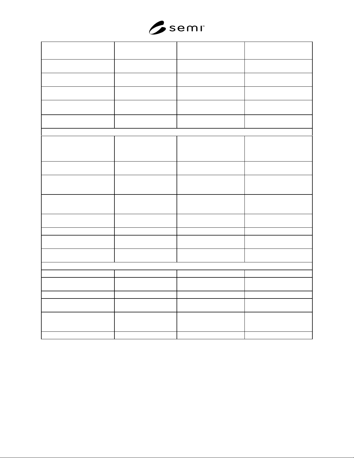
SEMI M41-1101 © SE MI 2000, 2001 4 Parameters (Units) V alue AS TM Test Method or Meas ureme nt Procedure Accepta nce Surface Roughn ess (nm) No te A, C AFM (SEMI M34) Note A, C Carrier Lifetime (µsec) Note C µ-P CD Meth…
SEMI M41-1101 © SEMI2000, 20013
5.1.3 Buried oxide thickness and thickness tolerances
5.1.4 Top silicon film thickness and thickness
tolerances
5.1.5 Warp limits
5.1.6 Top silicon film OSF defect limits
5.1.7 Top silicon film carrier life time limits
5.1.8 Buried oxide defect limits
5.1.9 Edge profile of the top silicon film and non-SOI
edge area
5.1.10 Rotation alignment between top silicon film and
the base silicon
5.1.11 Position of the bonding interface
5.1.12 Methods of test and measurements (see
Sections 8 and 9)
5.1.13 Lot acceptance procedures (see Section 7)
5.1.14 Certification (if required)
5.1.15 Packing and marking (see Section 10)
NOTE 2: Verification test procedures of certification of these
items shall be agreed upon between the users and the supplier
(see Sections 8 and 9).
6 Requirements
6.1 The complete specifications for Overall Wafer, Top
Silicon Film, Buried Oxide (BOX) and Base Silicon
Wafer are listed in Tables 1 to 5.
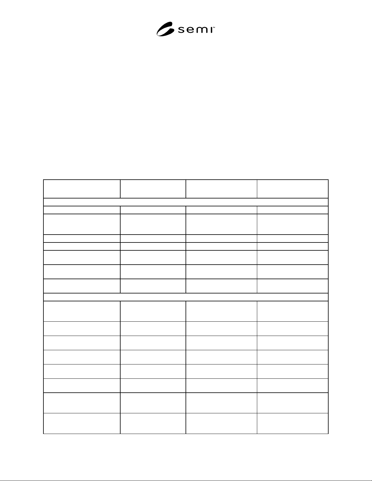
Table 1 Silicon-on-Insulator (SOI) Specifications for Low Voltage (45–60V) Power Device (1)
Parameters (Units) Value ASTM Test Method or
Measurement Procedure
Acceptance
Wafer(Overall)
Diameter (mm) 125, 150, 200 F613-93 Note A
Thickness (µm) (Value of regular silicon
wafer) + (SOI thickness) +
(Box thickness)
F533-96, F1530-94 Note A
Total Thickness Variation (µm) Note C F1530-94 Note C
LTV (µm) Note C F1530-94 Note C
Warp (µm) ≤ 100 (Note B, C, F) F1390-92 Note C, or Certified by
Wafer Manufactures
Non-SOI Edge Area (mm) ≤ 3 (Note C) Optical Metrology Note C, or Certified by
Wafer Manufactures
Edge Profile/Edge Profile
Surface Finish
Note C F928-93 Note C, or Certified by
Wafer Manufactures
Top Silicon Film
Thickness (µm) 2–12 Note D
(F399-88)
Note C, E,
Must be measured on each
wafer
Surface Orientation Note C X-ray Diffraction
(F26-87a)
Note C, or Certified by
Wafer Manufactures
Resistivity (ohm-cm) Note C F43-93, F84-93,
F1527-94
Note C, or Certified by
Wafer Manufactures
Conductivity Type Note C F42-93 Note C, or Certified by
Wafer Manufactures
Oxygen Concentration (/cm
3
) Note C F1188-93a,
F1619-95
Note C, or Certified by
Wafer Manufactures
Carbon Concentration (/cm
3
) Note C F1391-93 Note C, or Certified by
Wafer Manufactures
Surface Cleanliness: Metal
Contamination (/cm
2
)
Note A, C AAS, ICP-MS,
TXRF (F1526-95),
SIMS (F1617-98)
Note A, C
Surface Cleanliness: Particle
Density (/wafer)
Note A, C Light Scattering
Tomography (F1620-96)
(SEMI M34)
Note A, C
SEMI M41-1101 © SEMI 2000, 2001 4
Parameters (Units) Value ASTM Test Method or
Measurement Procedure
Acceptance
Surface Roughness (nm) Note A, C AFM
(SEMI M34)
Note A, C
Carrier Lifetime (µsec) Note C µ-PCD Method
(F1535-94)
Note C
Crystalline Alignment of Top
Silicon Film to Base Wafer (°)
Note C X-ray diffraction
(F847-94)
Note C
Surface Feature
(Haze, Scratch, etc)
None F154-94, F523-93,
F1726-97
Must be measured on each
wafer
OSF Density (/cm
2
) Note C Optical Metrology
(F1727-97)
Note C, or Certified by
Wafer Manufactures
Buried Oxide (BOX)
Thickness (µm) 0.5–2 Ellipsometry (F576-95)
or
Reflective Spectroscopy
(SEMI M34)
Tolerance is ± 5%; Note C,
or Certified by Wafer
Manufactures
Location of Bonded Interface Lower Surface
(Note C)
TEM Certified by Wafer
Manufactures
Void Density (/cm
2
) None Scanning Acoustic
Tomography, Optical Defect
Inspection
Note C
Oxide Defect Density (/cm
2
) Note C I-V on Capacitor,
Cu Decoration
(SEMI M34)
Note C
Dielectric Breakdown Voltage
(V)
Note C I-V on Capacitor Note C
Interface States (/cm
2
) Note C, H C-V Technique Note C
Fixed Charge Density (/cm
2
) Note C, H C-V Technique
(F1153-92)
Note C
Bonding Strength (kg/cm
2
) Note C Tensile Strength Note C, or Certified by
Wafer Manufactures
Base Silicon Wafer
Crystalline Orientation Note C F26-87a Note C
Resistivity (ohm-cm) Note C F43-93, F84-93,
F1527-94
Note C
Conductivity Type Note C F42-93 Note C
Fiducial Axis Orientation
(Flat/Notch)
Note C F671-90, F1152-93 Note C
To-be-bonded Surface
Cleanliness: Metals (/cm
2
)
Note C AAS, ICP-MS,
XRF (F1526-95),
SIMS (F1617-98)
Note C
Back Surface Finish Note C Optical Metrology Note C
SEMI M41-1101 © SEMI2000, 20015
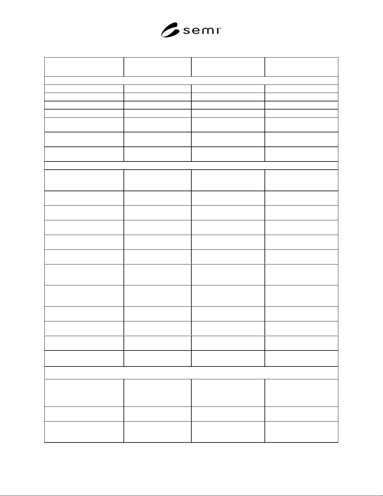
Table 2 Silicon-on-Insulator (SOI) Specifications for Low Voltage (45–60V) Power Device (2)
Parameters (Units) Value ASTM Test Method or
Measurement Procedure
Acceptance
Wafer(Overall)
Diameter (mm) 125, 150, 200 F613-93 Note A
Thickness (µm) Note A F533-96, F1530-94 Note A
Total Thickness Variation (µm) Note C F1530-94 Note C
LTV (µm) Note C F1530-94 Note C
Warp (µm)
≤ 50 (Note B, C, F)
F1390-92 Note C, or Certified by
Wafer Manufactures
Non-SOI Edge Area (mm)
≤ 3 (Note C)
Optical Metrology Note C, or Certified by
Wafer Manufactures
Edge Profile / Edge Profile
Surface Finish
Note C F928-93 Note C, or Certified by
Wafer Manufactures
Top Silicon Film
Thickness (µm) 0.1–0.5 Note D Note C, E,
Must be measured on each
wafer
Surface Orientation Note C X-ray Diffraction
(F26-87a)
Note C, or Certified by
Wafer Manufactures
Resistivity (ohm-cm) Note C F43-93, F84-93,
F1527-94
Note C, or Certified by
Wafer Manufactures
Conductivity Type Note C F42-93 Note C, or Certified by
Wafer Manufactures
Oxygen Concentration (/cm
3
) Note C F1188-93a,
F1619-95
Note C, or Certified by
Wafer Manufactures
Carbon Concentration (/cm
3
) Note C F1391-93 Note C, or Certified by
Wafer Manufactures
Surface Cleanliness: Metal
Contamination (/cm
2
)
Note A, C AAS, ICP-MS,
TXRF (F1526-95),
SIMS (F1617-98)
Note A, C
Surface Cleanliness: Particle
Density (/wafer)
Note A, C Light Scattering
Tomography (F1620-96)
(SEMI M34)
Note A, C
Surface Roughness (nm) Note A, C AFM
(SEMI M34)
Note A, C
Carrier Lifetime (µsec) Note C µ-PCD Method
(F1535-94)
Note C
Crystalline Alignment of Top
Silicon Film to Base Wafer (°)
Note C X-ray Diffraction
(F847-94)
Note C
Surface Feature
(Haze, Scratch, etc)
None F154-94, F523-93, F1726-97
(SEMI M34)
Must be measured on each
wafer
Buried Oxide (BOX)
Thickness (µm) 0.4–1.0 Ellipsometry (F576-95)
or
Reflective Spectroscopy
(SEMI M34)
Tolerance is ± 5%;
Note C, or Certified by
Wafer Manufactures
Location of Bonded Interface Lower Surface
(Note C)
TEM Certified by Wafer
Manufactures
Void Density (/cm
2
) None Scanning Acoustic
Tomography, Optical Defect
Inspection
Note C