semi合集-English.pdf - 第5831页
SEMI P29-0997 © SEMI 1997 3 Figure 6 Shifter Area Transmittance 5 Mask St ructure 5.1 Stru ct ure of a sh i fter shall be s p e cified as single- layer type or multilayer type. A halftone shifter film whose com ponents g…
SEMI P29-0997 © SEMI 1997 2
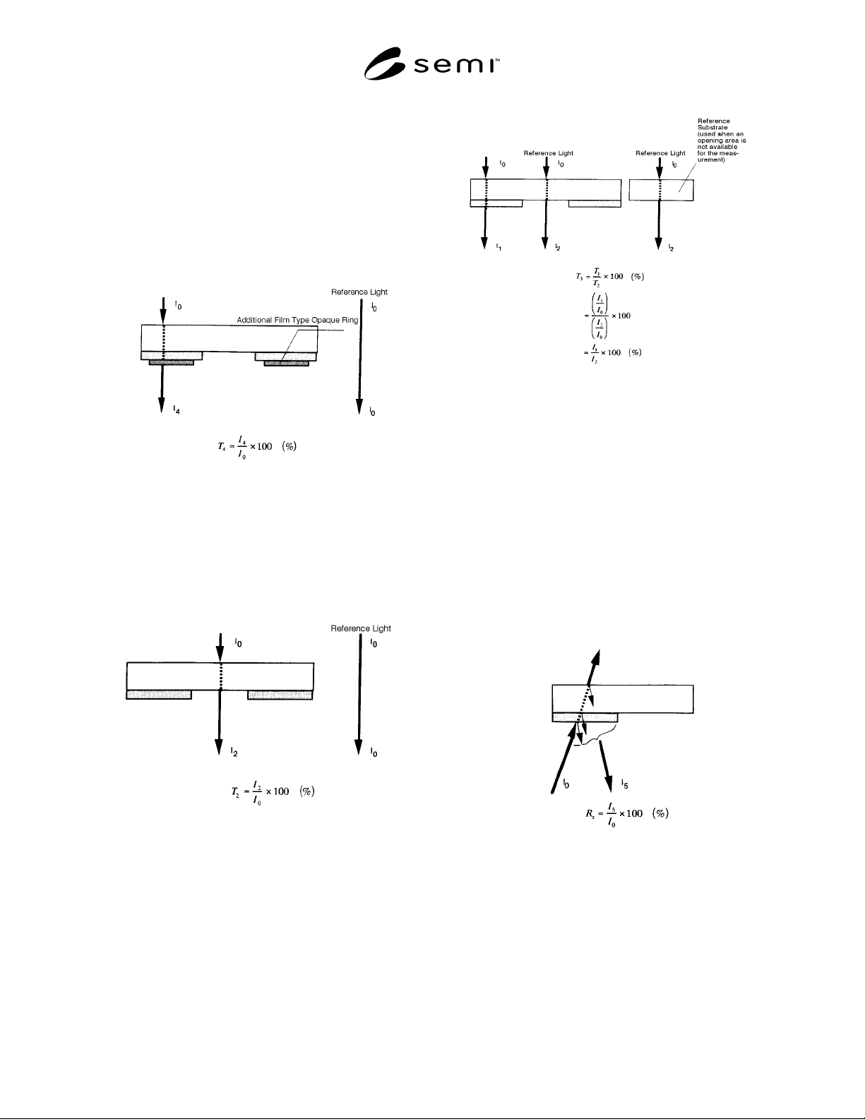
4.3.2 opaque ring transmittance — a ratio of intensity
of light transmitted through the additional film type
opaque ring area to intensity of incident light measured
with air reference. (Figure 2 illustrates the opaque ring
transmittance.)
NOTE 1: For a halftone phase shift mask with embedded
shifter type opaque ring, transmittance of the opaque ring area
is not defined in this guideline because it depends heavily on
the characteristics of the optical systems used.
Figure 2
Opaque Ring Transmittance
4.3.3 opening area transmittance — a ratio of
intensity of light transmitted through an opening area of
a patterned halftone phase shift mask to intensity of
vertical incident light measured with air reference.
(Figure 3 illustrates the opening area transmittance.)
Figure 3
Opening Area Transmittance
4.3.4 phase difference — a difference in phase of light
generated by vertical transmission through a shifter area
and an opening area with air equivalent to the shifter
film in thickness.
4.3.5 relative transmittance — a ratio of intensity of
light transmitted through a shifter area to intensity of
light transmitted through an opening area. (Figure 4
illustrates the relative transmittance.)
Figure 4
Relative Transmittance
4.3.6 shifter side reflectivity — a ratio of intensity of
reflected light to intensity of incident light onto the
surface of a shifter film. The reflected light is the sum
of the reflected light from the shifter surface and
reflected light from the boundary between shifter and
glass, and the boundary between glass and air. The
reflectivity depends on the incident angle, the
wavelength of the light, and the extent of polarization
of the incident light. The intensity of incident light is
usually calculated by the intensity of reflected light
measured using reference mirror. (Figure 5 illustrates
the shifter side reflectivity.)
Figure 5
Shifter Side Reflectivity
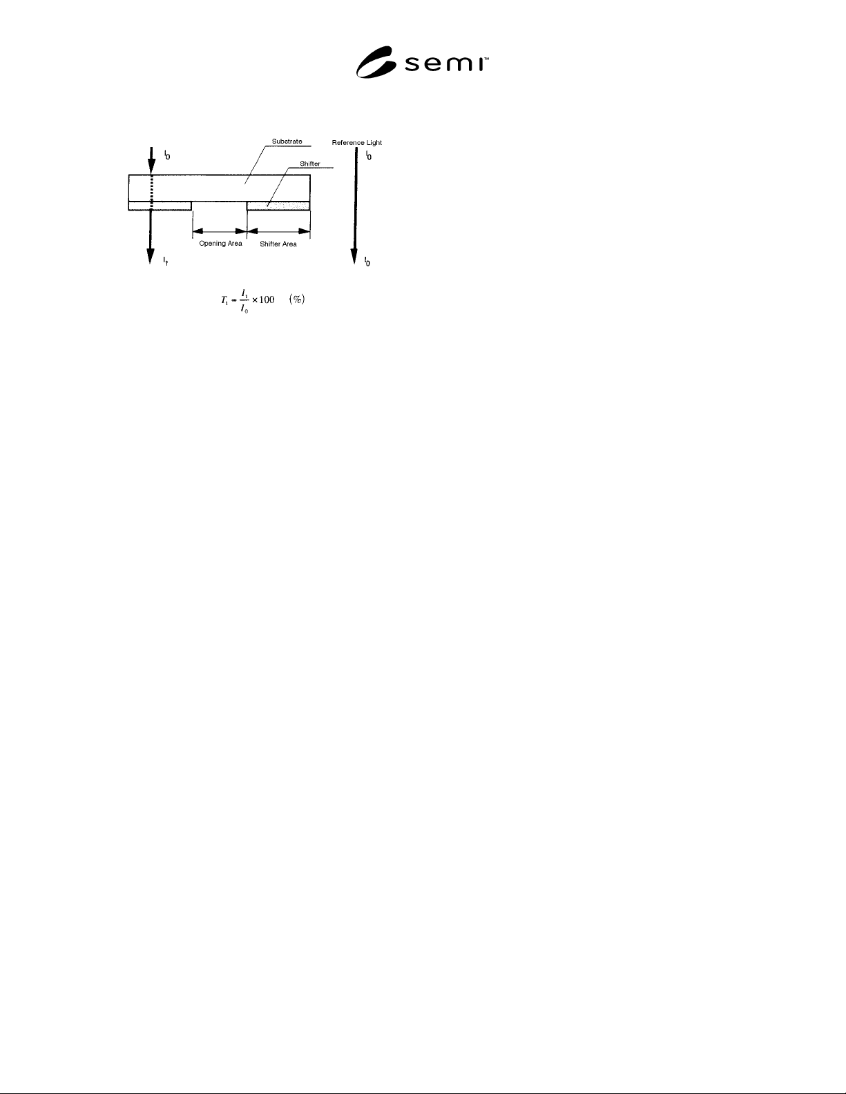
4.3.7 shifter area transmittance — ratio of intensity of
light transmitted through a shifter area of a halftone
phase shift mask (blank) to intensity of vertical incident
light measured with air reference. (Figure 6 illustrates
the shifter transmittance.)
SEMI P29-0997 © SEMI 19973
Figure 6
Shifter Area Transmittance
5 Mask Structure
5.1 Structure of a shifter shall be specified as single-
layer type or multilayer type. A halftone shifter film
whose components gradually change is classified into
the multilayer type.
5.2 Structure of an opaque ring shall be specified as
embedded shifter type or additional film type. In case of
a mask blank, a light shield film may be added or not.
5.3 Addition of an electrically conductive layer, and/or
a thin film for an etch-stop function shall be agreed
upon by the supplier and user.
6 Film Thickness
6.1 For a mask blank, specifications such as film
thickness of a shifter shall be agreed upon by the
supplier and user. The film thickness may be described
using a physical film thickness obtained from step
height measurement, an optical film thickness obtained
from ellipsometry or spectroscopy, and a controlled-
film thickness obtained from rate method. Measuring
method and measuring instrument shall be agreed upon
by the supplier and user.
7 Film Materials
7.1 Specifications for materials and composition per
layer in a shifter film and the opaque ring shall be
agreed upon by the supplier and user.
8 Exposure Wavelength
8.1 As exposure wavelength, the center wavelength of
g-line, i-line, KrF, ArF, and/or DUV shall be described
in nm.
9 Transmittance
9.1 Specifications of transmittance shall be agreed
upon by the supplier and user considering the selection
of terms listed in Section 4.3 of this guideline.
9.2 A relative transmittance can also be obtained from
the ratio of the shifter transmittance to the opening
transmittance of a patterned halftone phase shift mask.
In case the opening is not measurable, or it is a mask
blank, a transmittance of a reference substrate should be
used. The reference substrate shall be agreed upon by
supplier and user beforehand.
9.3 Specifications of opening transmittance shall be
agreed upon by the supplier and user considering its
dependency to etching method.
9.4 Transmittance at the defect inspection wavelength,
the dimension measurement wavelength, and/or the
alignment wavelength shall be agreed upon by the
supplier and user.
10 Phase Difference
10.1 Specifications of phase difference shall be agreed
upon by the supplier and user giving attention to the
measurement method. The unit should be degree. For a
mask blank, the dependency of phase difference of a
processed mask on the process method should be
considered.
10.2 A measurement wavelength should be specified
with its center value in nm. The measurement
instrument and the bandwidth shall be agreed upon by
the supplier and user.
11 Reflectivity
11.1 Shifter side reflectivity and glass side reflectivity
should be described in percent, and its specification
shall be agreed upon by the supplier and user. A
measuring wavelength, a measuring instrument, a
reference mirror, and an incident angle which are used
for measurement shall be agreed upon by the supplier
and user.
11.2 A defect inspection wavelength and an alignment
wavelength shall be agreed upon by the supplier and
user.
12 Opaque Ring Specificatio n
12.1 Specification of an opaque ring shall be agreed
upon by the supplier and user considering the type of
opaque ring.
SEMI P29-0997 © SEMI 1997 4
13 Etching Characteristics
13.1 Specifications of etching characteristics of a
mask blank shall be agreed upon by the supplier and
user.
14 Electrical Conductance
14.1 Electrical characteristics of a halftone phase shift
mask blank should be represented by sheet resistance,
and its specification and measuring method shall be
agreed upon by the supplier and user.
15 Defects
15.1 Specific defects of a halftone phase shift mask
and mask blank are phase defects and transmittance
defects.
These defects are caused by halftone shifter dot, half-
tone shifter hole, halftone shifter protrusion, halftone
shifter intrusion, halftone shifter film thickness defect,
halftone shifter film quality defect, and foreign
materials.
15.2 Specifications for inspection and repair shall be
agreed upon by the supplier and user.
15.3 Definition of defect sizes should conform to
SEMI P22.
16 Ordering Information
16.1 It is recommended to agree mutually on the
following items when ordering halftone phase shift
masks. The other items should conform to SEMI P1.
Type of halftone structure Single-layer type, or
multilayer type
Type of opaque ring Embedded shifter type, or
additional film type
Film materials To be agreed upon by the
supplier and user
Exposure wavelength To be agreed upon by the
supplier and user
Transmittance To be agreed upon by the
supplier and user
Phase difference To be agreed upon by the
supplier and user
Reflectivity To be agreed upon by the
supplier and user
Defects, foreign materials,
repair
To be agreed upon by the
supplier and user
16.2 It is recommended to agree mutually on the
following items when ordering halftone phase shift
mask blanks. The other items should conform to SEMI
P1.
Type of halftone structure Single-layer type, or
multilayer type
Light shield film Added, or not
Film materials To be agreed upon by the
supplier and user
Exposure wavelength To be agreed upon by the
supplier and user
Transmittance To be agreed upon by the
supplier and user
Phase difference To be agreed upon by the
supplier and user
Reflectivity To be agreed upon by the
supplier and user
Etching characteristics To be agreed upon by the
supplier and user
Electrical conductivity To be agreed upon by the
supplier and user
Defects, foreign materials To be agreed upon by the
supplier and user
17 Sampling
17.1 Sampling should conform to SEMI P1.
18 Related Documents
SEMI P3 — Specification for Photoresist/E-Beam
Resist for Hard Surface Photoplates
NOTICE: These standards do not purport to address
safety issues, if any, associated with their use. It is the
responsibility of the user of these standards to establish
appropriate safety and health practices and determine
the applicability of regulatory limitations prior to use.
SEMI makes no warranties or representations as to the
suitability of the standards set forth herein for any
particular application. The determination of the
suitability of the standard is solely the responsibility of
the user. Users are cautioned to refer to manufacturer’s
instructions, product labels, product data sheets, and
other relevant literature respecting any materials
mentioned herein. These standards are subject to
change without notice.
The user’s attention is called to the possibility that
compliance with this standard may require use of
copyrighted material or of an invention covered by
patent rights. By publication of this standard, SEMI
takes no position respecting the validity of any patent
rights or copyrights asserted in connection with any
item mentioned in this standard. Users of this standard
are expressly advised that determination of any such
patent rights or copyrights, and the risk of infringement
of such rights, are entirely their own responsibility.
Copyright by SEMI® (Semiconductor Equipment and Materials
International), 3081 Zanker Road, San Jose, CA 95134. Reproduction
of the contents in whole or in part is forbidden without express written
consent of SEMI.