semi合集-English.pdf - 第7370页
SEMI MF1392-1103 © SEMI 2003 14 m = number of individual val ues of net carrier den- sity to be averaged (s ee Section 12.5.1), k = whole number suc h that C i+k is between 80 and 85% of C i , n = number of ca pacitance-…

SEMI MF1392-1103 © SEMI 2003 13
12.3.1.3 Calculate and record the average depth, W
i
, in
µm, for each value of i from 1 to n − k as follows:
()()
()
1
1
−
⋅
′
−
′
′
−
′
=
+
+
iikii
S
i
S
ki
i
SWWS
WW
W
ii
(15)
where:
W
′
i
=
i
th
calculated depth, µm,
W
′
i+k
=
(i + k)
th
calculated depth, µm,
S
I
= i
th
dimensionless value calculated in Section
12.3.1.1,
k = whole number such that C
i+k
is between 80 and
85% of C
i
, and
n = number of measured capacitance-voltage pairs.
12.3.2 Calculate and record the net carrier density, N
i
,
in cm
−3
, corresponding to each average depth, W
i
, as
follows:
()
ikii
iki
i
WWW
VV
N
′
−
′
−
×=
+
+
14
10466.6
(16)
where:
V
i
= i
th
recorded voltage, V,
V
′
i+k
= (i + k)
th
recorded voltage, V,
W
i
′
=
i
th
calculated depth, µm,
W
′
i+k
=
(i + k)
th
calculated depth, µm, and
k = whole number such that C
i+k
is between 80 and
85% of C
i
.
12.3.3 Proceed to Section 12.5.
12.4 Curve-Fitting Method
12.4.1 Fit a polynomial of the following form
10
to the
capacitance-voltage pairs, C
i
− V
i
:
k
iki
i
fi
VaVa
Vaa
C
′
′
+++++
++=
)6.0()6.0(
)6.0(
1
2
2
10
2
K
(17)
where:
k
′
= order of the polynomial, chosen so that it
represents the lowest-order fit for which
| (C
i
′ − C
fi
)/C
i
′| ≤ 0.01 for all values of i and
for which k
′
≤ 10 or n − 1, whichever is
smaller (see Note 18).
n = number of capacitance-voltage pairs
determined in the test,
C
fi
= i
th
value of capacitance, pF, calculated fro
m
the fit,
a
0
... a
k
= coefficients determined such that the quan-
tity (C
i
′ − C
fi
)
2
summed over all values of i
is minimized,
10 Daniel, C., and Wood, F. S., Fitting Equations to Data (Wiley-
Interscience, New York, NY) 1971, p. 19.
C
′
i
= i
th
corrected capacitance, pF, and
V
i
= i
th
recorded (positive) voltage, V.
NOTE 18: Failure to meet this condition for a low-order
polynomial (k
′
≤ 3) may be caused by a single outlier; in such
cases, the polynomial should be redetermined without this
datum. Failure to meet this condition may also suggest that
the method is inappropriate for analysis of the data set; in
such cases, use of the incremental method is preferred.
12.4.2 Record the values of C
fi
and a
0
, a
1
, ... a
k
′
.
12.4.3 Calculate and record D
i
, the derivative of the
polynomial for 1/C
fi
2
with respect to diode voltage at
the depth appropriate to the i
th
voltage-capacitance pair,
as follows:
1
21
)6.0()6.0(2
−
′
+
′
++++=
k
iii
VkVaaD K (18)
where the other symbols are defined following Eq. 15.
12.4.3.1 Calculate and record the depletion depth, W
i
,
in µm, and the net carrier density, N
i
, in cm
−3
,
corresponding to each capacitance-voltage pair as
follows:
fi
eff
i
C
A
W
10359= (19a)
and
ieff
i
DA
N
2
7
102050.1 ×
−= (19b)
where:
A
eff
= mercury probe contact area, cm
2
, as determined
in Section 10.3.4,
C
fi
= the i
th
calculated capacitance, pF, and
D
i
= the derivative of the polynomial for 1/C
fi
2
with
respect to diode voltage at the depth W
i
.
12.5 Determine the average net carrier density as
follows:
12.5.1 Take the number of individual values of net
carrier density to be averaged as the number of values
that fall within the flat zone of the epitaxial layer or
within the depth range of the specimen over which the
average net carrier density is desired. Record this
number as m; m may not exceed n − k if the incremental
method was used for the calculations or n if the curve-
fitting method was used for the calculations.
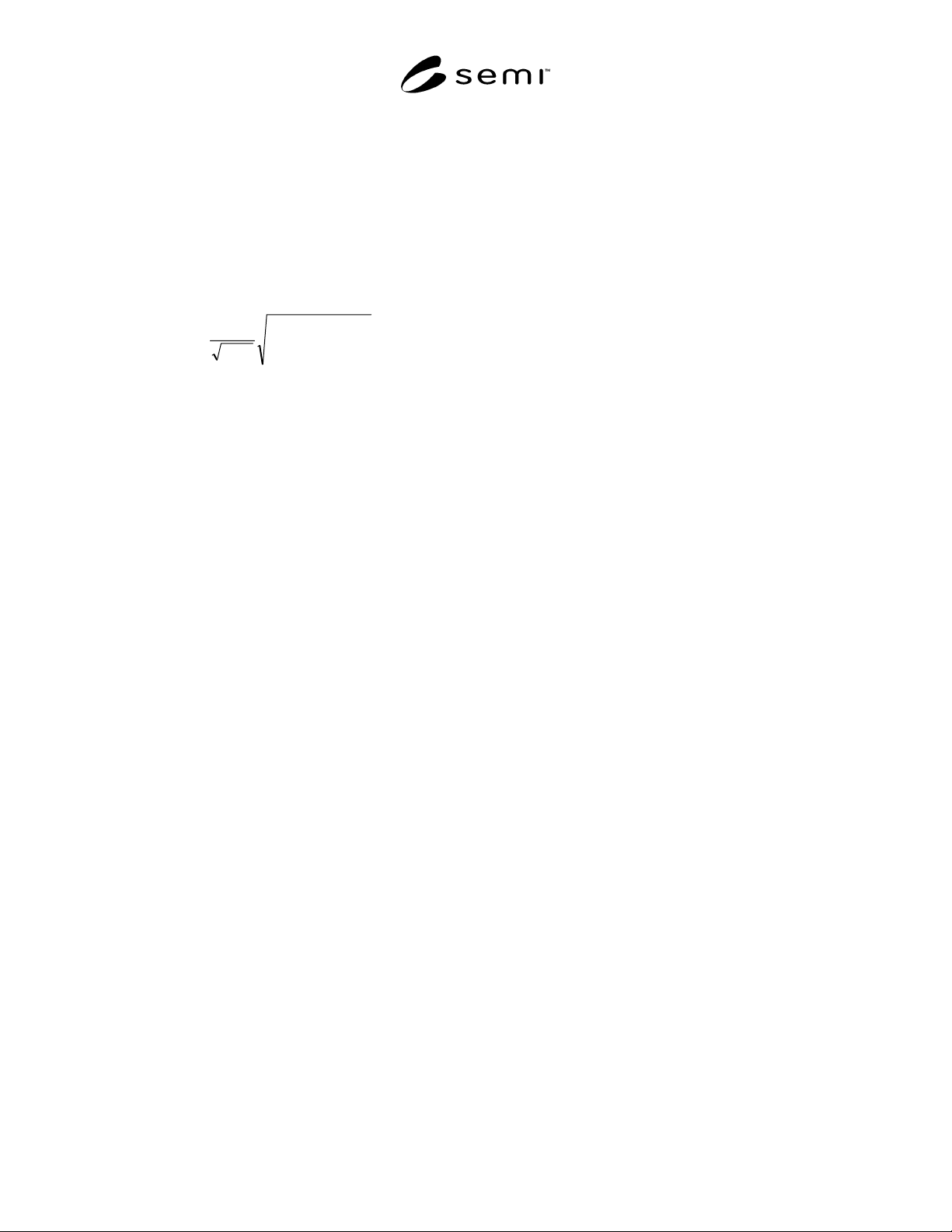
12.5.2 Calculate the average net carrier density, N
avg
, in
cm
−3
, as follows:
∑
=
=
m
i
iavg
N
m
N
1
1
(20)
where:
SEMI MF1392-1103 © SEMI 2003 14
m = number of individual values of net carrier den-
sity to be averaged (see Section 12.5.1),
k = whole number such that C
i+k
is between 80 and
85% of C
i
,
n = number of capacitance-voltage pairs measured,
and
N
i
=
net carrier density, cm
−3
, corresponding to each
average depth, W'
i
.
12.5.3 Calculate the sample standard deviation of the
net carrier density as follows:
∑
=
−
−
=
m
i
avgi
NN
m
s
1
2
)(
1
1
(21)
12.6 If the test wafer is not homogeneously doped or if
s exceeds 10% of N
avg
, plot the net carrier density
profile as a graph of N
i
as a function of W
i
.
NOTE 19: Related Information 3 describes composition of
the numerical constants used in the above calculations.
13 Report
13.1 Report the following information:
13.1.1 Type and model number of instrumentation used
including software type and revision, if a computer
controlled system is employed,
13.1.2 Probe configuration used,
13.1.3 Operator identification,
13.1.4 Date of measurement,
13.1.5 Lot number and test specimen identification
including conductivity type and surface orientation,
13.1.6 Wafer and sampling plan, if applicable,
13.1.7 Compensation capacitance, pF, as determined in
Section 10.2,
13.1.8 Method of calculation used, and
13.1.9 Average net carrier density, N
avg
, and sample
standard deviation, s, or net carrier density profile (plot
of N
i
as a function of W
i
), as determined in Section
12.5.
13.2 For referee measurements, also report the
following:
13.2.1 Mercury probe contact area, A
eff
, cm
2
, as
determined in Section 10.3.4,
13.2.2 Forward resistance at 1 V bias or equivalent
series resistance, Ω, as determined in Section 11.4,
13.2.3 Phase angle, degrees, as determined in Section
11.4.2.4, if measured,
13.2.4 Maximum applied reverse bias voltage, V, as
determined in Section 11.5,
13.2.5 Maximum leakage current density, J
r
, mA/cm
2
,
as determined in Section 11.5,
13.2.6 Surface treatment used, if applicable, and
13.2.7 Other data as tabulated in a data sheet
appropriate to the calculation method used.
14 Precision and Bias
14.1 Repeatability — The within-laboratory precision
achievable with this test method was estimated from
the results of several experiments. In the first
experiment, ten nominally 50 Ω·cm n-type wafers were
measured on two days by two different operators using
a single instrument. The pooled coefficient of variation
was 0.183%; the largest observed coefficient of
variation was 0.35%.
14.1.1 Based on the pooled value, the repeatability, r,
is estimated to be about 0.51%. In the second
experiment, ten nominally 1 Ω·cm n-type wafers were
measured three times on a single instrument by a single
operator. The wafer surfaces were treated prior to each
measurement. The pooled coefficient of variation was
0.493%; based on this value the repeatability, r, is
estimated to be about 1.37%.
14.2 Reproducibility — The reproducibility of this test
method has not been evaluated because of difficulties in
establishing and applying a common specimen surface
preparation for use in a round robin to evaluate
reproducibility. No such tests are planned.
14.3 Calculations of the errors in net carrier density, N
i
,
and depletion depth, W
i
, expected on the basis of the
precision requirements of the various parameters
measured in the test procedure could, in principle, be
made in accordance with the procedures of Practice
D 4356. However, because the formulas include ratios
of differences of both capacitance and voltage and
because the voltage and capacitance are coupled, these
errors depend both on the intervals chosen in the
experiment and on the physical characteristics of the
test specimen. The calculation procedure for the
incremental method included in this test method uses
large intervals in order to minimize the errors from the
use of finite intervals for the determination. For some
examples of the effect of both random errors and finite
interval errors on the calculated value of net carrier
density, N
i
.
9
14.4 Bias — The bias of this test method cannot be
evaluated because there are no available reference
standards suitable for evaluating bias.

SEMI MF1392-1103 © SEMI 2003 15
15 Keywords
15.1 capacitance-voltage method; carrier density;
carrier density profile; depth profile; epitaxial wafers;
mercury probe; net carrier density; polished wafers;
profiles; resistivity; silicon; single crystal silicon