semi合集-English.pdf - 第5253页
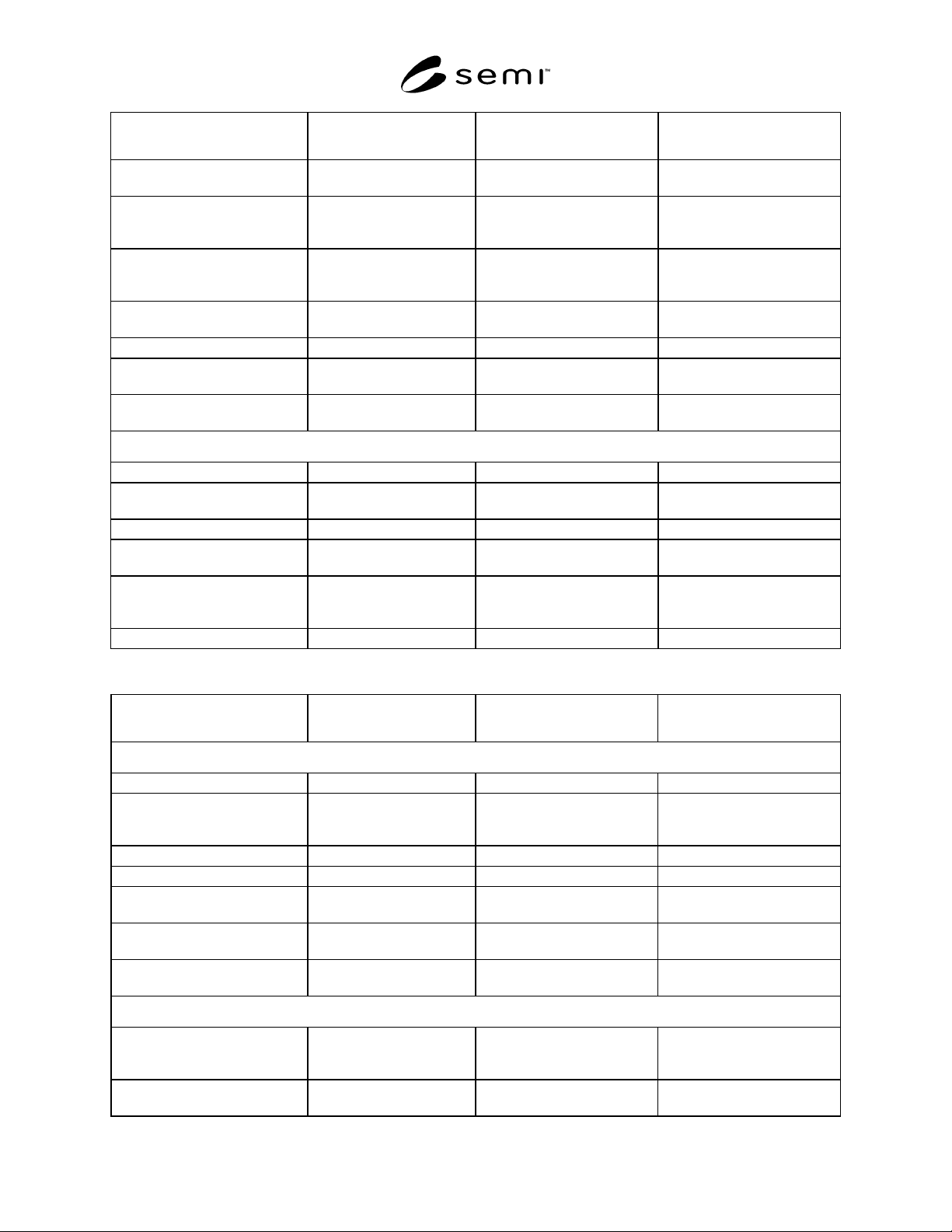
SEMI M41-1101 © SE MI 2000, 2001 10 Parameters (Units) V alue AS TM Test Method or Meas ureme nt Procedure Acceptanc e Resis tivity (ohm- c m) Note C F43-93, F 84-93, F1527- 94 Note C, or Ce rtified by Wafer Manufactures…
SEMI M41-1101 © SEMI2000, 20019
Parameters (Units) Value ASTM Test Method or
Measurement Procedure
Acceptance
Location of Bonded Interface Lower Surface, or
Inside Oxide
TEM Certified by Wafer
Manufactures
Void Density (/cm
2
) None Scanning Acoustic
Tomography, Optical Defect
Inspection
Note C
Oxide Defect Density (/cm
2
) Note C I-V on Capacitor,
Cu Decoration
(SEMI M34)
Note C
Dielectric Breakdown Voltage
(V)
Note C I-V on Capacitor Note C
Interface States (/cm
2
) Note C, H C-V Technique Note C
Fixed Charge Density (/cm
2
) Note C, H C-V Technique
(F1153-92)
Note C
Bonding Strength (kg/cm
2
) Note C Tensile Strength Note C, or Certified by
Wafer Manufactures
Base Silicon Wafer
Surface Orientation Note C F26-87a Note C
Resistivity (ohm-cm) Note C F43-93, F84-93,
F1527-94
Note C
Conductivity Type Note C F42-93 Note C
Fiducial Axis Orientation
(Flat/Notch)
Note C F671-90, F1152-93 Note C
To-be-bonded Surface
Cleanliness: Metals (/cm
2
)
Note C AAS, ICP-MS,
TXRF (F1526-95),
SIMS (F1617-98)
Note C
Back Surface Finish Note C Optical Metrology Note C
Table 5 Silicon-on-Insulator (SOI) Specifications for High Voltage (500–600V) Power Device
Parameters (Units) Value ASTM Test Method or
Measurement Procedure
Acceptance
Wafer(Overall)
Diameter (mm) 125, 150, 200 F613-93 Note A
Thickness (µm) (Value of regular silicon
wafer) + (SOI thickness) +
(Box thickness)
F533-96, F1530-94 Note A
Total Thickness Variation (µm) Note C F1530-94 Note C
LTV (µm) Note C F1530-94 Note C
Warp (µm)
≤ 100 (Note B,C,G)
F1390-92 Note C, or Certified by
Wafer Manufactures
Non-SOI Edge Area (mm)
≤ 3 (Note C)
Optical Metrology Note C, or Certified by
Wafer Manufactures
Edge Profile / Edge Profile
Surface Finish
Note C F928-93 Note C, or Certified by
Wafer Manufactures
Top Silicon Film
Thickness (µm) 3–17 Note D
(F399-88)
Note C, E,
Must be measured on each
wafer
Surface Orientation Note C X-ray Diffraction
(F26-87a)
Note C, or Certified by
Wafer Manufactures
SEMI M41-1101 © SEMI 2000, 2001 10
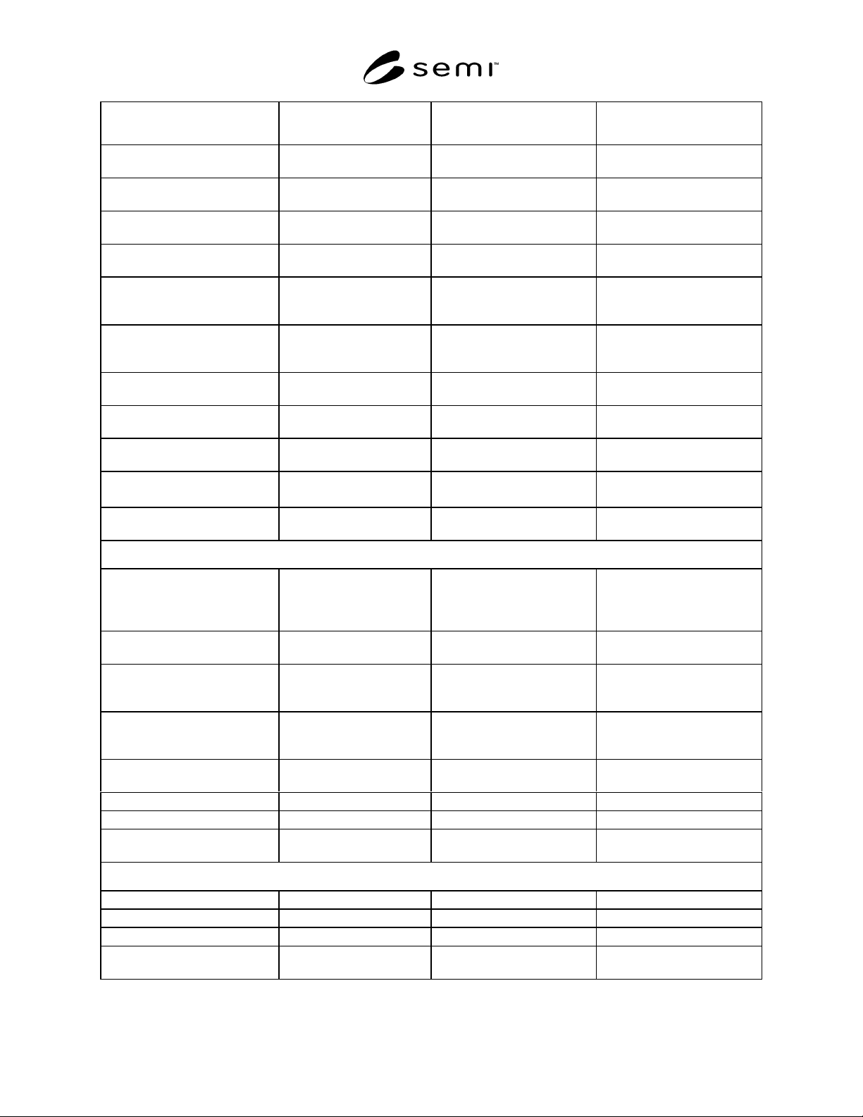
Parameters (Units) Value ASTM Test Method or
Measurement Procedure
Acceptance
Resistivity (ohm-cm) Note C F43-93, F84-93,
F1527-94
Note C, or Certified by
Wafer Manufactures
Conductivity Type Note C F42-93 Note C, or Certified by
Wafer Manufactures
Oxygen Concentration (/cm
3
) Note C F1188-93a,
F1619-95
Note C, or Certified by
Wafer Manufactures
Carbon Concentration (/cm
3
) Note C F1391-93 Note C, or Certified by
Wafer Manufactures
Surface Cleanliness: Metal
Contamination (/cm
2
)
Note A, C AAS, ICP-MS,
TXRF (F1526-95),
SIMS (F1617-98)
Note A, C
Surface Cleanliness: Particle
Density (/wafer)
Note A, C Light Scattering
Tomography (F1620-96)
(SEMI M34)
Note A, C
Surface Roughness (nm) Note A, C AFM
(SEMI M34)
Note A, C
Carrier Lifetime (µsec) Note C µ-PCD Method
(F1535-94)
Note C
Crystalline Alignment of Top
Silicon Film to Base Wafer (
o
)
Note C X-ray Diffraction
(F847-94)
Note C
Surface Feature
(Haze, Scratch, etc)
None F154-94, F523-93, F1726-
97
Must be measured on each
wafer
OSF Density (/cm
2
) Note C Optical Metrology
(F1727-97)
Note C, or Certified by
Wafer Manufactures
Buried Oxide (BOX)
Thickness (µm) 3–5 Ellipsometry (F576-95)
or
Reflective Spectroscopy
(SEMI M34)
Tolerance is ± 5%;
Note C, or Certified by
Wafer Manufactures
Location of Bonded Interface Inside Oxide
(Lower Surface)
TEM Certified by Wafer
Manufactures
Void Density (/cm
2
) None Scanning Acoustic
Tomography, Optical Defect
Inspection
Note C
Oxide Defect Density (/cm
2
) Note C I-V on Capacitor,
Cu Decoration
(SEMI M34)
Note C
Dielectric Breakdown Voltage
(V)
Note C I-V on Capacitor Note C
Interface States (/cm
2
) Note C, H C–V Technique Note C
Fixed Charge Density (/cm
2
) Note C, H C–V Technique (F1153-92) Note C
Bonding Strength (kg/cm
2
) Note C Tensile Strength Note C, or Certified by
Wafer Manufactures
Base Silicon Wafer
Surface Orientation Note C F26-87a Note C
Resistivity (ohm-cm) Note C F43-93, F84-93, F1527-94 Note C
Conductivity Type Note C F42-93 Note C
Fiducial Axis Orientation
(Flat/Notch)
Note C F671-90, F1152-93 Note C

SEMI M41-1101 © SEMI2000, 200111
Parameters (Units) Value ASTM Test Method or
Measurement Procedure
Acceptance
To-be-bonded Surface
Cleanliness: Metals (/cm
2
)
Note C AAS, ICP-MS,
TXRF (F1526-95),
SIMS (F1617-98)
Note C
Back Surface Finish Note C Optical Metrology Note C
Note A: Same as the standard of regular silicon wafer
Note B: The value is of 150 mm wafers, and is determined according to wafer diameter.
Note C: To be determined by negotiation between wafer users and suppliers
Note D: Reflective spectroscopy or FT-IR is recommended for top silicon film of less than several µm (about 7 µm), and FT-IR for top silicon
film of more than several µm (about 7 µm).
Note E: Tolerance of ± 0.5 µm is recommended for top silicon film of less than several µm (about 7 µm), and ± 1.0 µm for top silicon film of
more than several µm (about 7 µm).
Note F: The value is without the compensation method by backside oxide.
Note G: The value is with the compensation method by backside oxide.
Note H: This item can be neglected if the bonding interface is between BOX and base wafer.
7 Sampling Plan
7.1 Unless otherwise specified, ASTM Practice E 122
shall be used. When so specified, appropriate sample
sizes shall be selected from each lot in accordance with
ANSI/ASQC Z1.4. Each quality characteristic shall be
assigned an acceptable quality level (AQL) of lot
tolerance percent defective (LTPD) value in accordance
with ANSI/ASQC Z1.4 definitions for critical, major,
and minor classifications. If desired and so specified in
the contact or order, each of these classifications may
alternatively be assigned cumulative AQL or LTPD
values. Inspection levels shall be agreed upon between
the users and the suppliers.
8 Test Methods - Dimensions
NOTE 3: Detailed test procedures of each item should be
determined between the users and the suppliers.
8.1 Thickness of Top Silicon Film — The following
two methods are available for thickness measurement.
8.1.1 Reflective Spectroscopy — The light of visual
wavelength (400–800 nm) is introduced into top silicon
film by varying its wavelength continuously, and then
the reflective spectra is measured. When the light is
introduced into multi-layers of SOI wafers, reflection
occurs on the surface of top silicon film and the front
and backside of BOX. In such a case, the phase varies.
The final intensities of the light that reflects from top
silicon film surface are the sum of the intensity of light
that reflects from each layer. The thickness of top
silicon film and BOX makes optical path difference and
then results in phase difference that is dependent on its
wave length. The reflective light intensities, depending
on its wavelength, are measured. The reflective spectra
are defined as the ratio of reflective light intensity to
incident intensity. This spectra curve varies by the
thickness of top silicon film and BOX. The top silicon
film thickness is derived from the obtained spectra
curve by approximate calculation based on simulation
or by comparing with the database.
8.1.1.1 Reference: J.-P. Colinge, “Silicon-On-Insulator
Technology”, Kluwer Academic Publisher, 1991.
NOTE 4: Thickness of top silicon film and BOX layer are
limited to measure because of using visual light.
Example: Nanospec/AFT model : 210LCW, SP-FSC15
Top silicon film thickness: 0.01–15 µm
BOX thickness: 0.004–3 µm
NOTE 5: Optical constant is already known in each of
multilayers, and it should be constant in the whole layer.
8.1.2 FT-IR (Fourier Transform Infra-Red Spectro-
metry) — The reflectance spectrum of the specimen,
which exhibits successive maxima and minima
characteristics of optical interference phenomena, is
measured as a function of wavelength using an infrared
spectrophotometer. These maxima and minima are
observed when the optical path lengths of the infrared
beam, reflected from both the top silicon film surface
and the top silicon film–buried oxide interface, differ
by an integral number of half wavelengths.
Consequently, the thickness of top silicon film is
calculated using the wavelength of the extreme
maximum and minimum in reflectance spectrum, the
refractive index of Silicon and Silicon dioxide, and the
angle of incidence of the infrared beam upon the SOI
wafer.
Reference: F95 – Standard Test Method for Thickness
of Lightly Doped Silicon Epitaxial Layers on Heavily
Doped Silicon Substrates Using an Infrared Dispersive
Spectrophotometer
8.1.3 Definition of top silicon film thickness tolerance
— Thickness tolerance is defined below.
8.1.3.1 After top silicon film thickness is measured at
predetermined number of points within an SOI wafer,
the maximum and the minimum values are chosen, and
then the tolerance is defined as;