semi合集-English.pdf - 第7617页
Figure A1-1 Relationship Between the Maximum Siz e Matrix Code Symbol, Alphanumeric Fiel ds, and the Edges of the Polished Front Surface of Minimum Size Wafers SEMI T2-0298 © SEMI 1993, 2004 8

APPENDIX 1
SIMULTANEOUS MARKING WITH SQUARE DATA MATRIX AND
ALPHANUMERIC CODES
NOTICE: The material in this appendix is an official part of SEMI T2 and was approved by full letter ballot
procedures.
A1-1 The relative positions of alphanumeric and data matrix markings are shown in Figure A1-1. This figure also
shows the relationship between the data matrix code symbol and the edge of the polished area of the front surface of
the wafer. Wafer peripheries in the figure are the edges of the polished area of wafers with maximum intrusion of
the edge contour, minimum diameter, and maximum flat diameter (minimum flat length), or distance between the
notch pin centerline and the wafer edge, as specified in SEMI M1. For all wafer diameters, SEMI M1 allows the
edge contour to extend inward from the edge up to 508 µm (Dimension B in Figure 4 of SEMI M1). The distance
between the notch pin centerline and the wafer periphery may vary from 0.30 to 0.80 mm as indicated in Figure 6 of
SEMI M1. Other dimensions and tolerances are specified in the appropriate polished wafer specification in SEMI
M1.
A1-2 Alphanumeric code field locations are shown for all cases except the SEMI M13 code field for flatted wafers,
which lies entirely to the left of the primary fiducial bisector. Note that alphanumeric code field locations are not
specified for 125 mm diameter notched wafers in either SEMI M12 or SEMI M13.
A1-3 The nominal position of the reference point of the data matrix code symbol is marked by a +; this position is 1
mm to the right of the closest alphanumeric code field. Because of the tolerances on the position of the reference
point, the largest data matrix code symbol (20 × 20, 150 µm cell spacing) may lie anywhere within the dotted
square. The effect of a 3º skew toward the alphanumeric field is also shown. Although the skew does not affect
readability of the data matrix code symbol, too great a skew may cause the data matrix symbol code to impinge on
occupied areas of the wafer surface. The 3º skew, which is the maximum allowed by SEMI M12 and SEMI M13,
does not cause the data matrix code symbol to impinge on the alphanumeric code fields.
SEMI T2-0298 © SEMI 1993, 2004 7
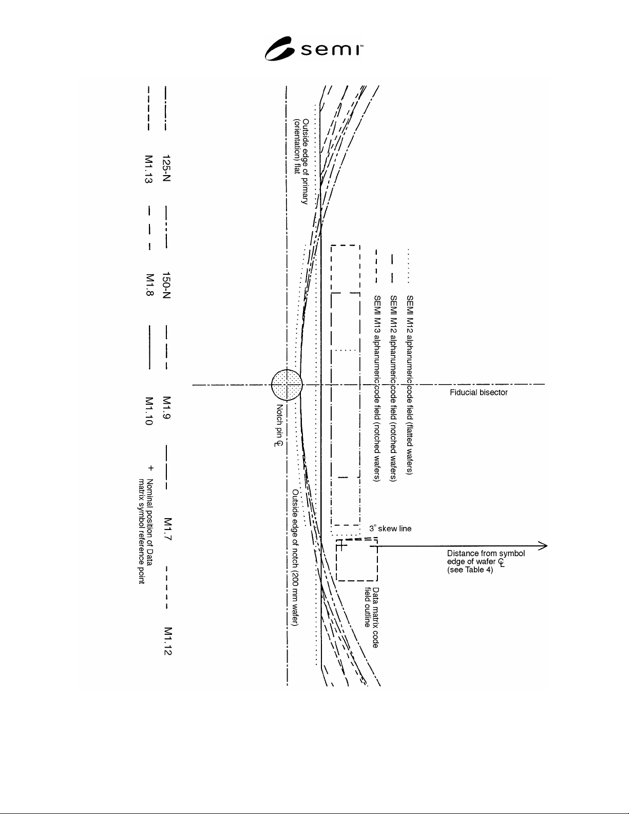
Figure A1-1
Relationship Between the Maximum Size Matrix Code Symbol, Alphanumeric Fields, and the Edges of the
Polished Front Surface of Minimum Size Wafers
SEMI T2-0298 © SEMI 1993, 2004 8

NOTICE: SEMI makes no warranties or representations as to the suitability of the standards set forth herein for any
particular application. The determination of the suitability of the standard is solely the responsibility of the user.
Users are cautioned to refer to manufacturer's instructions, product labels, product data sheets, and other relevant
literature, respecting any materials or equipment mentioned herein. These standards are subject to change without
notice.
By publication of this standard, Semiconductor Equipment and Materials International (SEMI) takes no position
respecting the validity of any patent rights or copyrights asserted in connection with any items mentioned in this
standard. Users of this standard are expressly advised that determination of any such patent rights or copyrights, and
the risk of infringement of such rights are entirely their own responsibility.
Copyright by SEMI® (Semiconductor Equipment and Materials
International), 3081 Zanker Road, San Jose, CA 95134. Reproduction of
the contents in whole or in part is forbidden without express written
consent of SEMI.
SEMI T2-0298 © SEMI 1993, 2004 9