semi合集-English.pdf - 第824页
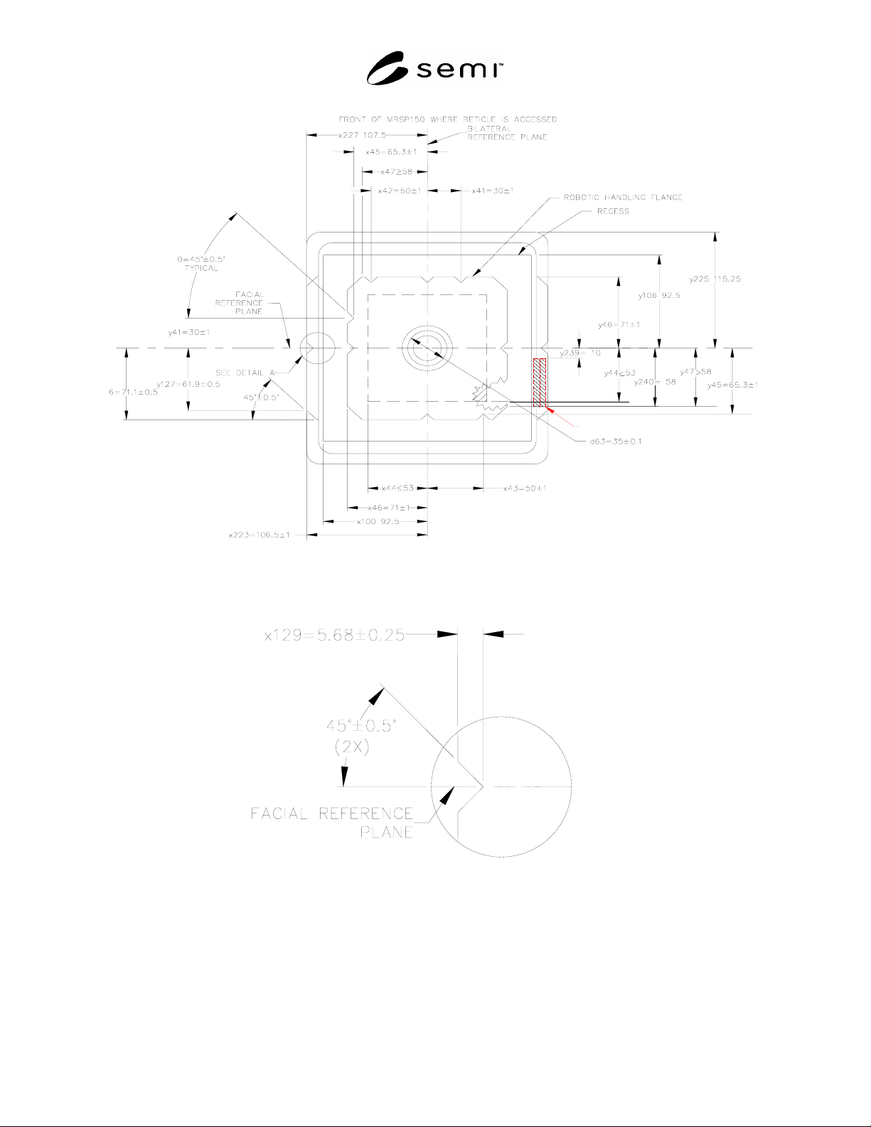
SEMI E112-0305 © SEMI 2001, 2005 6 RFID PLACEMENT ZONE Figure 1 External Top View of MRSP150 Figure 2 Detail A: Exte rnal Top View of Side Handling Flange Ali gnment Notch
SEMI E112-0305 © SEMI 2001, 2005 5
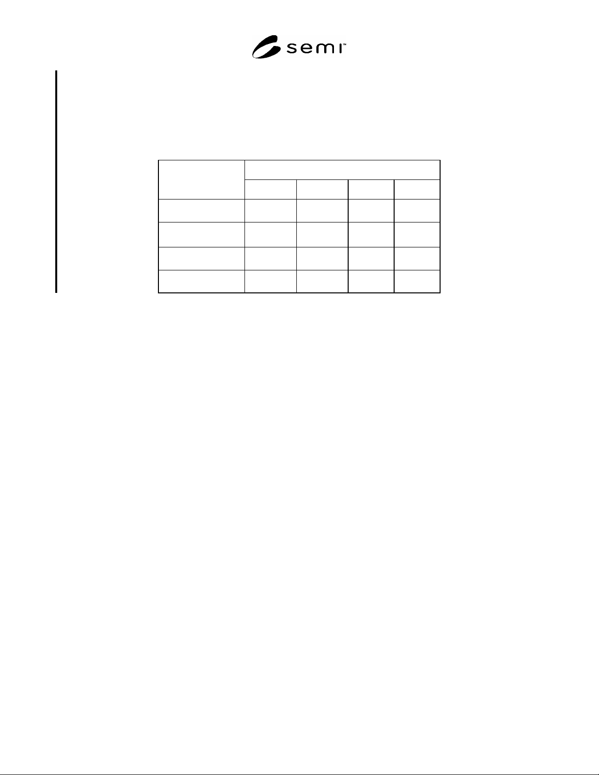
6.15 Info Pads — When the MRSP is placed on a port, the info pads A, B, C, and D communicate information
about the RSP configuration. Figure 10 shows the dimensions of the info pads. Table 2 defines the info pad
dimensions. A pad in the up position must be z26 above the horizontal reference plane. A pad in the down position
must be z2 above the horizontal reference plane. Info pad assignments are shown in Table 1. Info pads that are “not
defined” can be at either the up or down position unless specified by the end user. RSP configurations “to be
assigned” may be assigned by the end user.
Table 1
Info Pad
MRSP Configuration
A B C D
6 inch reticle not
defined
not
defined
up down
to be assigned not
defined
not
defined
down down
to be assigned not
defined
not
defined
up up
to be assigned not
defined
not
defined
down up
7 Related Documents
7.1 SEMI Standards
SEMI P1 — Specification for Hard Surface Photomask Substrates
SEMI S8 — Safety Guidelines for Ergonomics Engineering of Semiconductor Manufacturing Equipment
NOTICE: Unless otherwise indicated, all documents cited shall be the latest published versions.
SEMI E112-0305 © SEMI 2001, 2005 6
RFID PLACEMENT ZONE
Figure 1
External Top View of MRSP150
Figure 2
Detail A: External Top View of Side Handling Flange Alignment Notch
SEMI E112-0305 © SEMI 2001, 2005 7
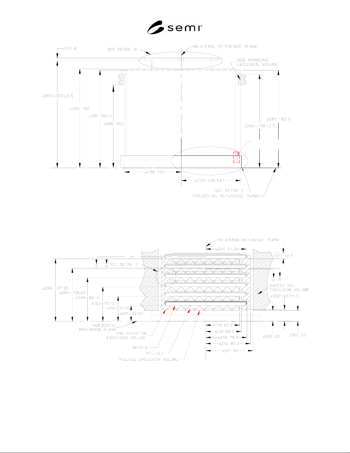
RFID PLACEMENT ZONE
Figure 3
External Rear View of MRSP150
Figure 4
Internal Front View of MRSP150