semi合集-English.pdf - 第6111页
SEMI G22-1296 © SE MI 1980, 1996 3 8 Defect Limits A magnification of 10 × to 30× shall be used to inspect the packages unl ess otherwise specified. 8.1 Ceramic 8.1.1 C racks — Per MIL-STD-883, M e thod 2009. 8.1.2 Chips…
SEMI G22-1296 © SEMI 1980, 1996 2
4.15 isolation gap — Metal-free space between
conductive areas.
4.16 layer — A dielectric sheet with or without
metallization that performs a discrete function as part of
the package.
4.17 peeling (flaking) — Any separation of
metallization from the base material that exposes the
base material.
4.18 pit — Any unspecified depression in the package.
4.19 projection — An adherent fragment of excess
parent material on the component surface.
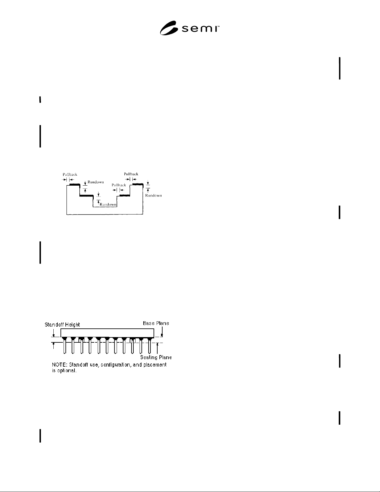
4.20 pullback — A dimension cove ring the linear
distance between the edge of the ceramic and the first
measurable metallization (see Figure 2).
Figure 2
Metallization Misalignment
4.21 rundown — The linear distance down a vertical
surface from the top to the point of maximum
metallization overhang (see Figure 2).
4.22 seal area — A dimensional outline area
designated for either metallization or bare ceramic to
provide a surface area for sealing.
4.23 seating plane — As defined by the standoff
features or the package base plane if no standoff is used
(see Figure 3).
Figure 3
Seating Plane
4.24 standoff — The designed separation between the
base plane and the seating plane created by a physical
feature. Standoff use, configuration, and placement is
optional (see Figure 3).
4.25 terminal — Metallization at the point of electri
cal contact to package internal circuitry.
4.26 TIR — Total indicator reading.
4.27 voids — An absence of refractory metallization,
braze, or plating material from a designated area greater
than 0.002" (0.051 mm) in diameter.
5 Ordering Information
Purchase orders for pin grid array packages furnished to
this specification shall include the following items:
1. Drawing number and revision level
2. Certification requirements
3. Quantity
4. Reference to this document
5. Any exceptions to print or specifications
6 Dimensions and Permissi ble Variations
The dimensions of the pin grid array package shall
conform to the SEMI Standards or to the customer
drawing and be within the outline of the appropriate
JEDEC standard. Refer to MIL-PRF-38535 and MIL-
STD-1835.
7 Material Parameters
The definitions, defects, and functional testing
described in this specification relate directly to a
nominal package made with the following materials.
They may also be applicable to similar pin grid array
packages made with other materials.
7.1 Ceramic Properties
7.1.1 Materials — Alumina content 90% minimum.
Beryllia content to be determined.
7.1.2 Color — Dark or white.
7.2 Metal Properties
7.2.1 Metallized circuits and areas shall be refractory
metal tungsten, molybdenum, or an approved
equivalent, 0.0003" (0.00762 mm) minimum thickness.
7.2.2 Finish shall be per MIL-PRF-38535 and MIL-
STD-1835; Nickel Plating (if designated) shall be per
QQ-N-290A, 50 µ"–350 µ" (0.0013 mm–0.00889 mm).
Gold plating shall conform to MIL-G-45204, Type III
and 50 µ"–225 µ" (0.0013 mm–0.00508 mm).
7.2.3 Braze shall be per MIL-STD-7883.
7.2.4 Pin Material — Iron nickel cobalt alloy per
MIL-PRF-38535 and MIL-STD-1835, Type A (Kovar).
Iron nickel alloy per MIL-PRF-38535 and MIL-STD-
1835, Type B (Alloy 42). Phosphor bronze per ASTM
B159.
SEMI G22-1296 © SEMI 1980, 19963
8 Defect Limits
A magnification of 10× to 30× shall be used to inspect
the packages unless otherwise specified.
8.1 Ceramic
8.1.1 Cracks — Per MIL-STD-883, Method 2009.
8.1.2 Chips — (See Figure 1.)
8.1.2.1 Edge — 0.100" (2.54 mm) length × 0.030"
(0.762 mm) width × 0.020" (0.508 mm) (see Figure 1,
A).
8.1.2.2 Corner — 0.030" (0.762 mm) length × 0.030"
(0.762 mm) width × 0.030" (0.762 mm) (see Figure 1,
B).
8.1.2.3 Chips cannot encroach upon contact pad or
expose any buried metallization.
8.1.2.4 Seal Area — 0.060" (1.52 mm) length × 0.020"
(0.508 mm) width × 0.020" (0.508 mm) depth
maximum.
8.1.2.5 Chips cannot reduce the seal width by more
than 1/3 of the design width.
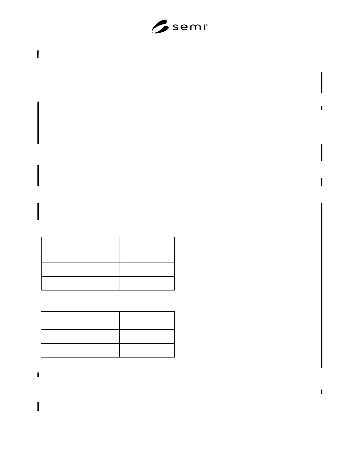
8.2 Package Flatness — 0.004 inch/inch (0.004
mm/mm) maximum.
8.2.1 Seal Area Flatness
Seal Area Size Seal Area Flatness (TIR)
0.000" – 0.500" (0 – 12.7 mm) 0.002" (0.51 mm)
Maximum
0.501" – 0.750" (12.72 – 19.05 mm) 0.003" (0.076 mm)
Maximum
0.751" & greater (19.07 mm) 0.004" (0.101 mm)
Maximum
8.2.2 Die Attach Area Flatness
Die Attach Area Flatness
Die Attach Area Flatness
(TIR)
0.000" – 0.500" (0 – 12.7 mm) 0.002" (0.051 mm)
Maximum
0.501" – 0.750" (12.72 – 19.05 mm) 0.0035" (0.088 mm)
Maximum
8.3 Metallization Voids — (Voids greater than 0.003"
(0.075 mm) should be considered.)
8.3.1 Seal Area — Maximum number of three (3)
voids per seal ring allowed. The maximum void
dimension is 0.010" (0.254 mm) and voids must be
separated by a minimum of 0.030" (0.762 mm).
8.3.2 Wire Bond Finger — Be free of voids or bare
spots in the bonding area as defined by customer
drawing.
8.3.3 Die Attach Area — Three (3) voids allowed,
maximum 0.010" (0.254 mm) diameter voids separated
by a distance greater than 0.010" (0.254 mm). Voids
within 0.015" (0.381 mm) of die attach cavity wall shall
not be considered as the basis for rejection.
8.3.4 Braze Metallization — A 0.010" (0.254 mm)
maximum diameter void is acceptable, one (1) void per
pad.
8.4 Metallization Misalignment — (See Figure 2.)
8.4.1 Metallization Rundown — Internal cavity not to
exceed 0.010" (0.254 mm) maximum.
8.4.2 Wire Bond Finger Pullback — 0.010" (0.254
mm) maximum.
8.4.3 Wire Bond Finger Rundown — Metallization
rundown not to exceed 0.010" (0.254 mm) maximum.
8.4.4 Pattern Isolation — Minimum shall not be
reduced by more than 50% of the design.
8.5 Pins
8.5.1 Pin Attachment — The pin must be within the
area of the braze pad (fillet seen on all sides). The pin
must be located within 0.010" (0.254 mm) radius of
true location with respect to all other pins.
8.5.2 Pins that are broken, missing, twisted, or bent
more than 30 °.
8.5.3 Pin burrs greater than 0.005" (0.125 mm) in any
direction.
8.6 Plating
8.6.1 Any visual evidence of plating defects such as
blistering, peeling, voids, or stains.
8.6.2 Any plating damage such as scratches or marred
areas that expose underlying base metal.
8.7 Components (General)
8.7.1 Any visual evidence of corrosion, contamination,
or chemical stains on the package component.
8.7.2 Any protrusion, conductive, or non-conductive,
that is more than 0.005" (0.125 mm) in height.
9 Sampling
Sampling size must meet the requirements of MIL-
STD-105 or MIL-PRF-38535 and MIL-STD-1835, or
as agreed to between vendor and customer. Single,
double or multiple samples may be used per vendor and
customer agreement.

SEMI G22-1296 © SEMI 1980, 1996 4
10 Test Methods
10.1 Mechanical, Electrical, and Thermal Test
Methods — Per MIL-STD-883 unless otherwise noted.
10.1.1 Gold plating and bake test of gold plated
package shall be tested by placing parts on a calibrated
heater per MIL-STD-883, Method 1008 (excluding
temperature).
10.1.1.1 Condition A — 450 ± 10°C for two minutes in
air, or
10.1.1.2 Condition B — 470 ± 10°C for one minute in
nitrogen.
10.1.1.3 After cooling at room temperature the
packages will be examined for the following criteria:
1. Blisters — None allowed at 10× magnification.
2. Any non-uniform color change of the gold at die
attach pad. Discolorations within edges up to 0.015"
(.381 mm) from the cavity wall is acceptable.
3. Any non-uniform color change of the bonding
fingers, seal ring surface, or external pins is not
acceptable.
4. There shall be no flaking or peeling of the package
plating when viewed at 10x magnification.
5. Superficial stains left during drying or prior
operations is not cause for rejection.
6. Plating adhesion tape test.
10.1.2 Lead Pull — Under the test condition of five (5)
pounds ± one-quarter (1/4) pound pull at an angle of
20° or less from the pins vertical line, measured
perpendicular to the package, there shall be no visible
separation of the braze joint under 10x magnification.
This excludes plating.
10.1.3 Lead Fatigue — Test per MIL-STD-883,
Method 2004, Test Condition B2, Section 3.1.
10.2 Functional Test Methods
10.2.1 Die Attach Quality — Destructive die shear test
post environmental testing per MIL-STD-883, Method
2019, Paragraph 3.2C.
10.2.2 Wire Bond Quality — Minimum pre-seal and
post-seal bond strength test per MIL-STD-883, Method
2011, Test Condition D. Reject for bonds which cause
plating to lift from the base metal of the bonding fingers
or fail to meet minimum strength requirement.
10.2.3 Solderability — Test per MIL-STD-883,
Method 2003 (omit aging).
10.2.4 Insulation Resistance — Test per MIL-STD-
883, Method 1003, Condition D.
10.2.5 Hermetic and Environmental Testing per MIL-
STD-883.
10.2.5.1 The hermetic integrity of the package must be
maintained after all environmental testing. Hermetic
checks shall comply with MIL-STD-883, Method 1014,
Test Conditions A, B, C, or D.
10.2.5.2 Environmental testing shall include but not be
limited to the following:
1. Temperature Cycle — MIL-STD-883, Method
1010, Condition C without heat sink; Condition B
with heat sink.
2. Thermal Shock — MIL-STD-883, Method 1011,
Condition C without heat sink; Condition B with
heat sink.
3. Centrifuge — MIL-STD-883, Method 2001,
Condition E. Y1 axis only — cavity up; Y2 axis
only — cavity down (optional).
4. Mechanical Shock — MIL-STD-883, Method 2002,
Condition B.
5. Vibration — MIL-STD-883, Method 2007,
Condition A.
NOTE 1: Package applications requiring a heat sink attach
will require the environmental test requirements (temp. cycle,
shock, etc.) to be evaluated on an individual basis. The
material, form factor, and method of attach used for heat sinks
may result in severe stresses being induced on the package
assembly during environmental testing. Actual accelerated
test requirements should be based on the expected product
application environment and may be less rigorous than those
tests for packages without heat sinks.
11 Sequence of Events and I ncoming Testing
During incoming inspection the sequence of testing
shall be:
A. Visual
B. Dimensional
C. Functional (typical functional tests which may be
applied):
Die Attach
Wire Bond
Pre-seal wire pull
Seal
Heat sink attach (if applicable)