semi合集-English.pdf - 第5053页
SEMI M20-1104 © SEMI 1991, 2004 2 coordinate sy stem. F urther, in SEMI E5 , the coor dinate system axes do not rotate; the wafer rotates with respect to these axes. In the wafer coordinate system, the coordinate axes ar…

SEMI M20-1104 © SEMI 1991, 2004 1
SEMI M20-1104
PRACTICE FOR ESTABLISHING A WAFER COORDINATE SYSTEM
This practice was technically approved by the Global Silicon Wafer Committee and is the direct
responsibility of the North American Silicon Wafer Committee. Current edition approved by the North
American Regional Standards Committee on August 16, 2004. Initially available at www.semi.org
September 2004; to be published November 2004. Originally published in 1991; previously published in
2004.
1 Purpose
1.1 Processing systems now employed in advanced
device manufacturing use aligning mechanisms to
position the wafer rotationally and in x-y prior to
processing. Many of these scan the wafer periphery
and determine the geometric center of the wafer
surface. This is most often seen on stepping aligners, to
minimize the effects of wafer-to-wafer diameter
variation in mixed aligner type fabs. Similar center-
referencing subsystems are found on many
characterization systems. The wafer coordinate system
provides a method for referencing any other coordinate
system, such as a site, pattern, or mapping array, to the
physical geometry of the wafer surface.
1.2 If the points of the array lie on the front surface of
the wafer, only the x and y (or r and θ) coordinates are
relevant. It has become increasingly important in
semiconductor material and device manufacturing to
describe, in unambiguous terms, the position of a point
on a wafer that automatic processing, test, or
characterization equipment can recognize and locate.
For example, characterization equipment needs to
report the precise locations of defects and anomalies
discovered in wafers before or after processing in order
to relate the presence or absence of such defects and
anomalies to device yield variations. The wafer
coordinate system can be used to establish the
coordinates of each point of interest, and, through
transformation to the yield analysis coordinate system,
relate them to the die yield map.
1.3 In response to these needs, this practice defines a
wafer coordinate system to facilitate the precise
locating and reporting of points on the wafer surface. If
the point or points lie above or below the surface, the z-
coordinate must also be used. Because the zero point
on the z-axis is application specific, this practice treats
the x-y-z (or r-
-z) system separately from the surface
coordinate system.
2 Scope
2.1 This practice covers procedures for defining a
wafer coordinate system for locating uniquely any point
on a wafer surface using the wafer center as the origin
and either Cartesian (x-y) or polar (r-θ) coordinates.
2.2 For unpatterned wafers, this wafer coordinate
system can be used directly or in conjunction with a
rectangular or polar overlay array.
2.3 This wafer coordinate system can also be used to
locate the origins or other reference points of other
coordinate systems used to define or report position
data of site, die, or map arrays on the front or back
surface of a patterned or unpatterned wafer. In this
way, the array coordinate system may be referenced to
the physical geometry of the wafer. Selected modes of
application of the wafer coordinate system are given for
information only in Related Information 1.
2.4 This practice also covers procedures for defining a
three-dimensional x-y-z (or r-
-z) coordinate system for
the wafer.
NOTICE: This standard does not purport to address
safety issues, if any, associated with its use. It is the
responsibility of the users of this standard to establish
appropriate safety and health practices and determine
the applicability of regulatory or other limitations prior
to use.
3 Limitations
3.1 Mask alignment conventions are not necessarily
consistent with the wafer coordinate system.
3.2 In SEMI M1, the position of the secondary flat on
silicon wafers is defined by the clockwise rotation from
the primary flat. This is opposite to the convention
used for the polar angle in the wafer coordinate system.
3.3 Also in SEMI M1, the coordinate system for the
edge profile template is, unlike the wafer coordinate
system, edge referenced. In addition, the edge profile
template uses the x coordinate for the radial direction
(positive from the wafer edge inward) and the y
coordinate for the vertical direction (positive from the
wafer surface toward the median plane of the wafer).
3.4 In SEMI E5, the “normal” position of the wafer is
defined similarly to that in the wafer coordinate system;
that is, the primary fiducial is downward and its
bisector is the negative y-axis. However, the rotational
position of the wafer is defined by its clockwise
rotation from the “normal” position, again opposite to
the convention used for the polar angle in the wafer

SEMI M20-1104 © SEMI 1991, 2004 2
coordinate system. Further, in SEMI E5, the coordinate
system axes do not rotate; the wafer rotates with respect
to these axes. In the wafer coordinate system, the
coordinate axes are referenced to the wafer itself,
independent of the physical position of the wafer in
space.
3.5 SEMI M12 and SEMI M13 specify the mark field
location for 100 mm, 125 mm, or 150 mm diameter
flatted wafers relative to the flat rather than the wafer
center. Thus, the mark field location may vary with
respect to the wafer center and the coordinates of the
corners of the mark field location (in the wafer
coordinate system) may vary from wafer to wafer.
However, the mark field location for notched wafers
150, 200, and 300 mm in diameter is referenced to the
wafer center.
3.6 There are some circumstances in which the front
surface of an unpatterned wafer is not readily
distinguished from the back surface.
4 Referenced Standards
4.1 SEMI Standards
SEMI E5 — SEMI Equipment Communications
Standard 2 Message Content (SECS-II)
SEMI M1 — Specifications for Polished
Monocrystalline Silicon Wafers
SEMI M12 — Specifications for Serial Alphanumeric
Marking of the Front Surface of Wafers
SEMI M13 — Specification for Alphanumeric Marking
of Silicon Wafers
SEMI M17 — Guide for a Universal Wafer Grid
NOTICE: Unless otherwise indicated, all documents
cited shall be the latest published versions.
5 Terminology
5.1 None.
6 Summary of Practice
6.1 Front Surface Coordinate System
6.1.1 The wafer is positioned with its front surface up.
6.1.2 The wafer center is located.
6.1.3 A right-handed Cartesian coordinate system is
erected.
6.1.4 The primary fiducial is located to be in the
negative y-direction.
6.1.5 Cartesian or polar coordinates (referenced to the
positive x-axis) are chosen according to the intended
application.
6.2 Back Surface Applications
6.2.1 The wafer is rotated about the bisector of the
primary fiducial (y-axis) until the back surface is up.
6.2.2 This reverses the direction of the x-axis, but
otherwise the back surface coordinate system is the
same as the front surface coordinate system.
6.3 Three-dimensional Coordinate System
6.3.1 Because the zero point on the z-axis is
application specific, only the direction of the z-
axis is
defined and the various possibilities for locating the
zero point are considered.
7 Procedure for Establishing Wafer
Coordinate Systems
7.1 Front Surface Coordinate System
7.1.1 Position the wafer front surface up.
7.1.2 Find the center of the wafer surface.
7.1.2.1 For purposes of this document, the periphery of
a wafer is assumed to be the smallest circle enclosing
the wafer, disregarding fiducials and all other edge
anomalies. Use the center of this circle as the center of
the wafer surface.
7.1.3 Erect a right-handed Cartesian coordinate system
with:
7.1.3.1 its origin at the center of the wafer surface,
7.1.3.2 the y-axis on the diameter in the plane of the
front surface which bisects the primary fiducial (flat or
notch), and
7.1.3.3 the x-axis on the diameter in the plane of the
front surface which is perpendicular to the bisector of
the primary fiducial (y-axis).
7.1.4 Orient the wafer so the primary fiducial is in the
negative y-direction (see Figure 1).
7.1.5 Take as the usual convention that the negative y-
direction is pointing downward (on a page) or toward
the operator (on a table or chuck or in a wafer carrier),
and that the positive x-axis points toward the right.
7.1.6 Reference the polar coordinates, r and θ to the
positive x-axis where
22
yxr (see Figure 1).
7.1.7 Choose Cartesian or polar coordinates according
to the application.
7.2 Back Surface Coordinates
7.2.1 Rotate the wafer around the bisector of the
primary fiducial (y-axis) until the back surface is up.
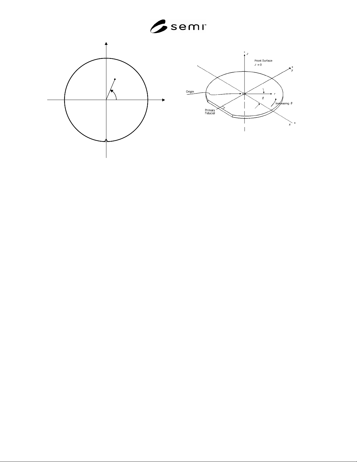
SEMI M20-1104 © SEMI 1991, 2004 3
x
y
(x
1
, y
1
)
(R
1
,
1
)
1
x
y
(x
1
, y
1
)
(R
1
,
1
)
1
x
y
(x
1
, y
1
)
(R
1
,
1
)
1
NOTE: The primary fiducial may be a flat or a notch.
Figure 1
Front Surface Coordinate System
7.2.2 With the primary fiducial in the negative y
direction (downward or toward the operator), the
positive x-axis points toward the left. In this way the x-
y-coordinates of a point on the back surface are the
same as the x-y coordinates of the point directly through
the wafer on the front surface.
7.3 Three-dimensional Coordinates
7.3.1 Place the wafer with the front surface up.
7.3.2 Erect the z-axis through the center of the wafer
surface and perpendicular to the plane of the surface
with the positive direction above the front surface (see
Figure 2).
7.3.3 Assign the zero point of the z-axis in accordance
with the application.
7.3.3.1 For example, for geometric measurements,
such as warp, the center of the z-axis may be at the
geometrical center of the wafer in three dimensions.
7.3.3.2 For front surface flatness measurements, the
zero point of the z-axis is usually taken at the reference
plane, which is chosen in accordance with the particular
flatness parameter being determined.
7.3.3.3 Other applications may require locating the
center of the z-axis at a different position.
7.3.3.4 For thickness or thickness variation
measurements, the zero point of the z-axis may be taken
at the center of the back surface of the wafer.
NOTE: The primary fiducial may be a flat or a notch.
Figure 2
Wafer Coordinate System with z-axis Direction
Indicated