semi合集-English.pdf - 第7597页
SEMI MF2166-0304 © SEMI 2004 10 RELATED INFORMATION 1 CORONA SUBSYSTEMS NOTICE: This related in formation is not an offi cial part of SEMI MF2166. It was develo ped during the original development of the docum ent. This …
SEMI MF2166-0304 © SEMI 2004 9
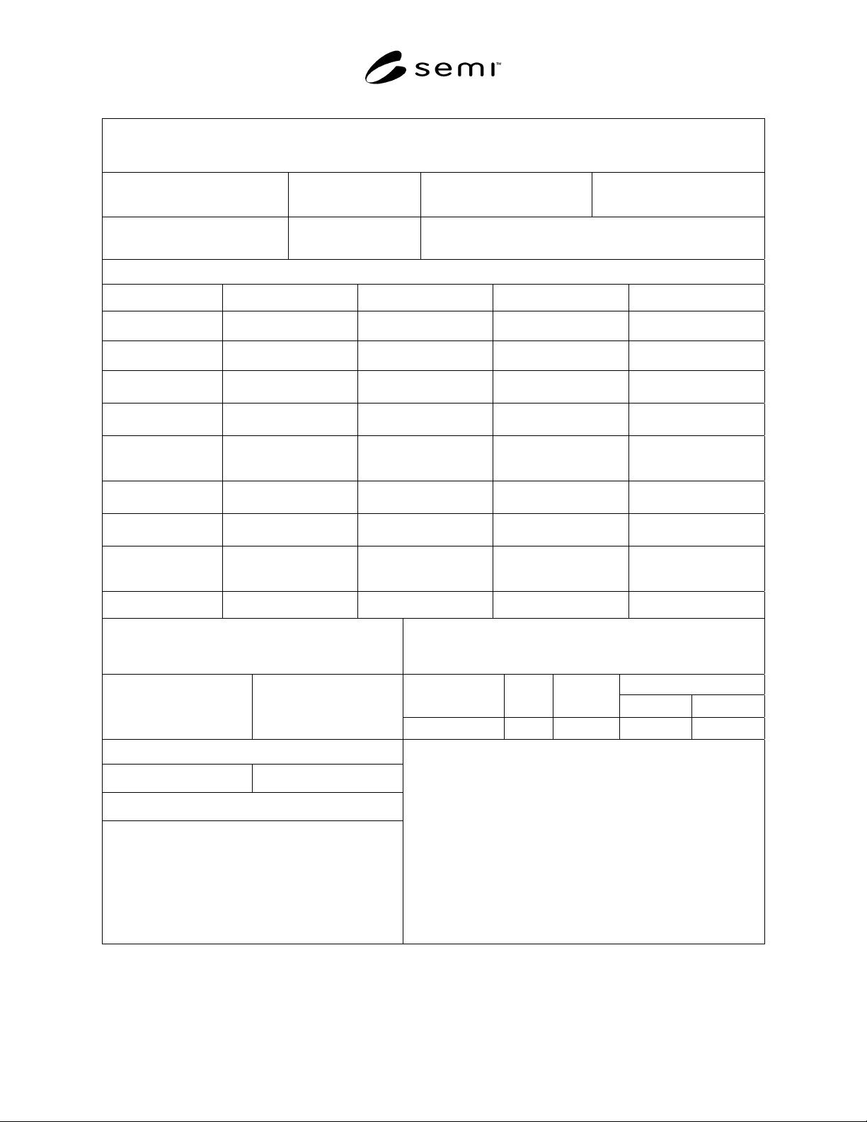
Special Reference Wafer Calibration Data Sheet For
Non-Contact Dielectric Characterization System
System Supplier: System Model #:
System Software Rev: Test Date:
Calibration Organization
Operator ID Method C — Line Source Corona [ ]
Measurement Data Statistics
Parameter
Mean
Std Dev (1 sigma) Minimum Maximum
V
cpd,
(V)
Corona Voltage per
Sweep
(−) CTS Voltage
(−) CTS Time
(−) CTS
Temperature
(+) CTS Voltage
(+) CTS Time
(+) CTS
Temperature
Q
m
(× 10
11
charge/ cm
2
)
Environmental Data
Special Reference Wafer Used
Calibration Dates
Serial Number Mfg.
Wafer
Dia.
Last Next
Temperature
_____ [ ]°F____ [ ]°C
Relative Humidity
Equipment Performance Summary
In Tolerance [ ] Out of Tolerance [ ]
Repair Required Yes [ ] No [ ]
Comments
Figure 2
Example Data Sheet for Method C
SEMI MF2166-0304 © SEMI 2004 10
RELATED INFORMATION 1
CORONA SUBSYSTEMS
NOTICE: This related information is not an official part of SEMI MF2166. It was developed during the original
development of the document. This related information was approved for publication by full letter ballot on October
16, 2003.
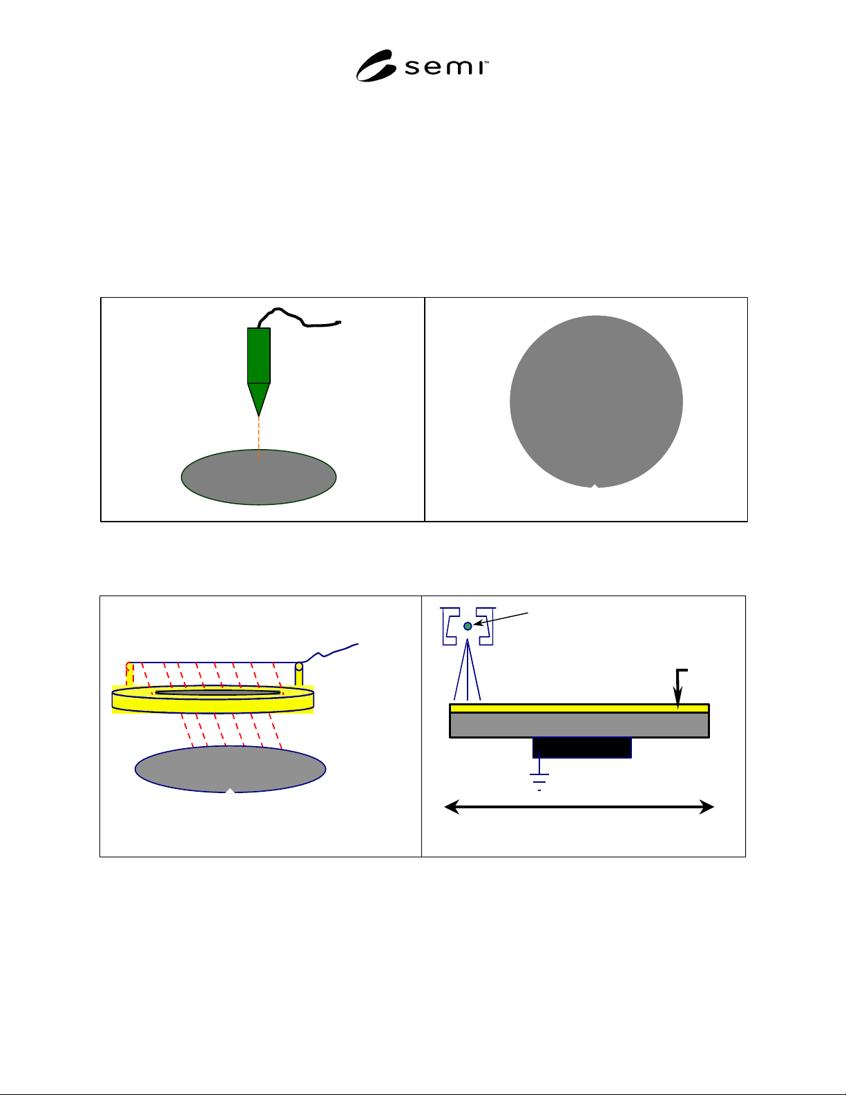
R1-1.1 Two types of coronas are used in NCDCSs:
R1-1.2 Point Source Corona — This corona type
applies charge at discrete locations on the wafer
surface. The area of the corona is defined by a mask.
(See Figure R1-1.)
R1-1.3 Line Corona — In this corona, a wire applies a
charge uniformly across the entire wafer. The charge
level is applied in increments that cause a V
cpd
change
of between 0.3 and 0.6 V. (See Figure R1-2.)
High
Voltage
Wafer
Linear Sam
p
lin
g
+
+
+
Figure R1-1
Point Corona – Method A
High
Voltage
Corona Wire
Wafer
High Voltage
Corona Wire
x
-motion
A
rea Scannin
g
Silicon
Chuc
k
Oxide
+ + + + + + + + + + +
Figure R1-2
Wire Corona – Method B and C

SEMI MF2166-0304 © SEMI 2004 11
NOTICE: SEMI makes no warranties or representations as to the suitability of the standards set forth herein for any
particular application. The determination of the suitability of the standard is solely the responsibility of the user.
Users are cautioned to refer to manufacturer's instructions, product labels, product data sheets, and other relevant
literature, respecting any materials or equipment mentioned herein. These standards are subject to change without
notice.
By publication of this standard, Semiconductor Equipment and Materials International (SEMI) takes no position
respecting the validity of any patent rights or copyrights asserted in connection with any items mentioned in this
standard. Users of this standard are expressly advised that determination of any such patent rights or copyrights, and
the risk of infringement of such rights are entirely their own responsibility.
Copyright by SEMI® (Semiconductor Equipment and Materials
International), 3081 Zanker Road, San Jose, CA 95134. Reproduction o
f
the contents in whole or in
p
art is forbidden without express written
consent of SEMI.