semi合集-English.pdf - 第7720页
SEMI T11-0703 © SEMI 2002, 2003 5 Pellicle Frame Pellicle mi salignment ( ± 0.5) } Area of Unpatterned Chrome Film 6.0 ( End Effector ) Reticle misalignm ent ( ± 1.5 ) 0.7 8.8 14.0 (nomina l) (Edge Exclusi on) Quiet Zone…
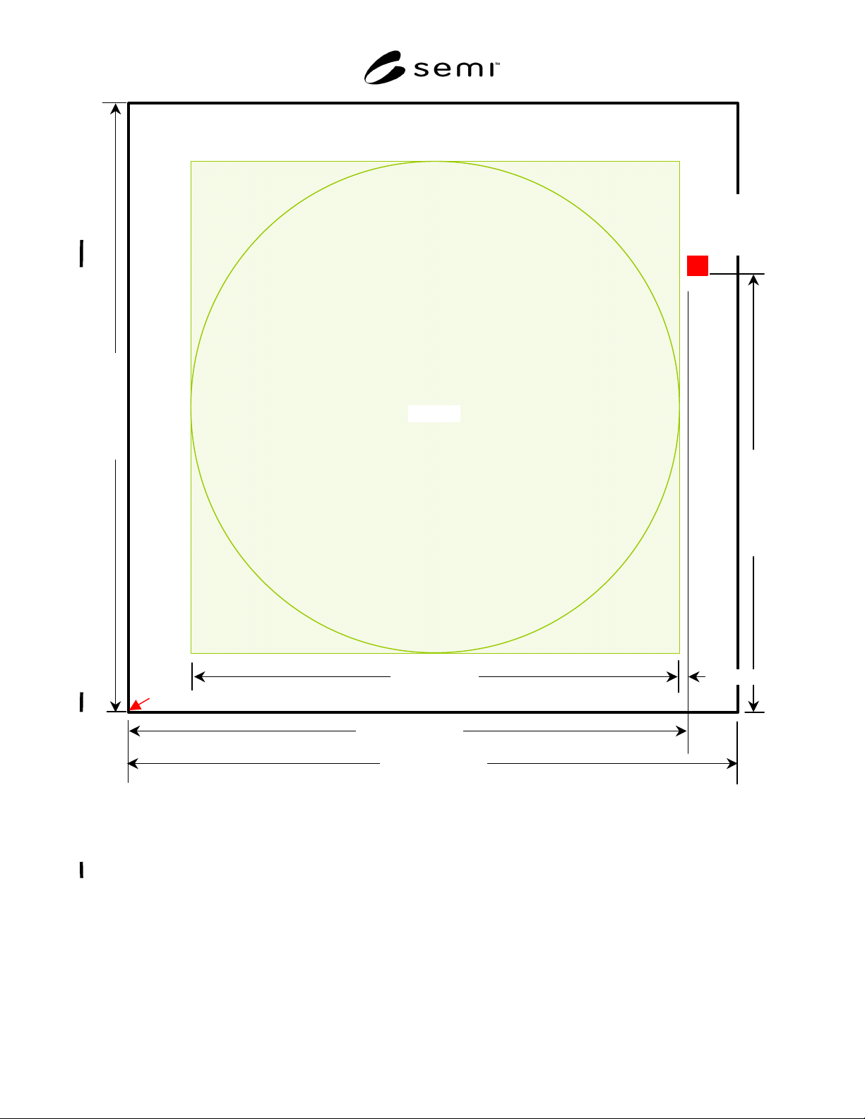
SEMI T11-0703 © SEMI 2002, 2003 4
139.6
±
0.5
152.0
±
0.4
11
0
.4
±
0
.
5
1
5
2.
0
±
0
.4
124 (nominal)
1.6
±
0.7
Pellicle
Substrate Reference Corner
Data Matrix
Code Symbol
(see detail in
Figure 3)
NOTE: All dimensions in millimeters.
Figure 2
Location of Data Matrix Code Symbol in Reticle Substrate Edge Exclusion Area
(Nominally 14 mm Wide)
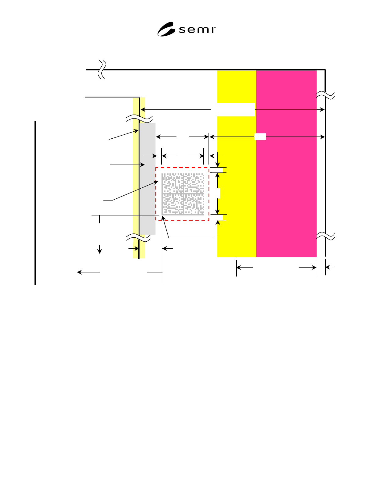
SEMI T11-0703 © SEMI 2002, 2003 5
Pellicle
Frame
Pellicle misalignment (±0.5)
}
Area of
Unpatterned
Chrome Film
6.0
(
End Effector
)
Reticle
misalignment
(
±
1.5
)
0.7
8.8
14.0 (nominal)
(Edge Exclusion)
Quiet Zone
139.6 ± 0.5 to
Substrate
Reference Corner
(see Figure 2)
110.4 ± 0.5 to
Substrate Reference
Corner (see Figure 2)
1.6
±
0.7
4.0
3.2
0.4
0.4
Data Matrix
Symbol Code
Reference
Corner
0.4
3.2
0.4
NOTE: All dimensions in millimeters.
Figure 3
Detail of Location of Data Matrix Code Symbol with Allowed Clearances to Related Elements
(see Related Information 1, Other Considerations, for Description of these Elements)
NOTICE: SEMI makes no warranties or representations as to the suitability of the standards set forth herein for any
particular application. The determination of the suitability of the standard is solely the responsibility of the user.
Users are cautioned to refer to manufacturer' s instructions, product labels, product data sheets, and other relevant
literature respecting any materials mentioned herein. These standards are subject to change without notice.
The user’s attention is called to the possibility that compliance with this standard may require the use of copyrighted
material or of an invention covered by patent rights. RVSI Acuity CiMatrix has filed a statement with SEMI
asserting that the patented or copyrighted item can be used by the public for the purpose of implementing this
standard without specific license and without payment of royalty or other charge. Attention is also drawn to the
possibility that some elements of this standard may be subject to patented technology or copyrighted items other
than those identified above. Semiconductor Equipment and Materials International (SEMI) shall not be held
responsible for identifying any or all such patented technology or copyrighted items. By publication of this
standard, SEMI takes no position respecting the validity of any patent rights or copyrights asserted in connection
with any item mentioned in this standard. Users of this standard are expressly advised that determination of any
such patent rights or copyrights and the risk of infringement of such rights are entirely their own responsibility.
SEMI T11-0703 © SEMI 2002, 2003 6
RELATED INFORMATION 1
OTHER CONSIDERATIONS
NOTICE: This related information is not an official part of SEMI T11. It was derived from task force discussions
and is provided for reference and information only. This related information was approved for publication by full
letter ballot on August 29, 2002.
R1-1 Other Considerations
R1-1.1 This specification defines only the location of
the ID mark on the reticle surface. However, issues
relating to substrate edge length tolerances, pellicles,
reticle positioning, robotic end effectors and alignment
marks were considered in development of the
specification. These are summarized below and in
Figure R1-1.
R1-1.2 Substrate Edge Length — Table 1 of SEMI P1
specifies that edge length for 6” reticle substrates shall
be ≥ 151.6 mm and ≤ 152.4 mm. Figure 2 represents
this as 152.0 ± 0.4 mm.
R1-1.3 Pellicles — It is assumed that the pellicle is a
square with a nominal size of 124 mm that is centered
on the mask substrate. A pellicle misalignment
allowance of ± 0.5 mm has been suggested by reticle
suppliers and users; this is reflected in Figure 3. An
unpatterened chrome film is specified between the quiet
zone and pellicle frame to eliminate influence on the
reader of light scattered from the pellicle frame when
mark reading illumination and the reader camera are on
opposite sides of the reticle as shown in Figure R1-1.
Effector End
Illuminator
CCD
Camera
Symbol
Pellicle
Reticle
Controller &
Decoder
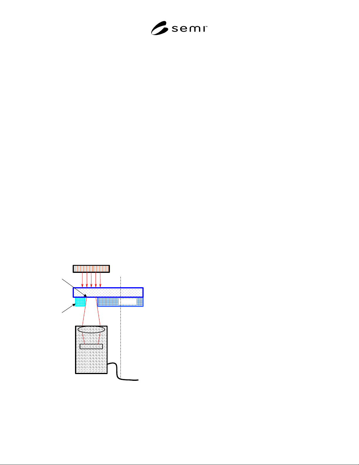
Figure R1-1
Example of Top-Side ID Illumination with Pattern-
Side Reader and End Effector
R1-1.4 Reticle Positioning — Misalignment in a tool
can result from several factors, e.g. position in the
cassette, position on the end effector, substrate
squareness and others. A reticle misaligment allowance
of ± 1.5 mm has been suggested by stepper and other
tool suppliers and users. This is reflected in Figure 3.
R1-1.5 Robotic End Effectors — End effector grips are
typically ≤ 6.0 mm wide, in the reticle contact area. A
6.0 mm end effector width is shown in Figure 3.
NOTICE: SEMI makes no warranties or
representations as to the suitability of the standards set
forth herein for any particular application. The
determination of the suitability of the standard is solely
the responsibility of the user. Users are cautioned to
refer to manufacturer' s instructions, product labels,
product data sheets, and other relevant literature
respecting any materials mentioned herein. These
standards are subject to change without notice.
The user’s attention is called to the possibility that
compliance with this standard may require the use of
copyrighted material or of an invention covered by
patent rights. RVSI Acuity CiMatrix has filed a
statement with SEMI asserting that the patented or
copyrighted item can be used by the public for the
purpose of implementing this standard without specific
license and without payment of royalty or other charge.
Attention is also drawn to the possibility that some
elements of this standard may be subject to patented
technology or copyrighted items other than those
identified above. Semiconductor Equipment and
Materials International (SEMI) shall not be held
responsible for identifying any or all such patented
technology or copyrighted items. By publication of this
standard, SEMI takes no position respecting the validity
of any patent rights or copyrights asserted in connection
with any item mentioned in this standard. Users of this
standard are expressly advised that determination of
any such patent rights or copyrights and the risk of
infringement of such rights are entirely their own
responsibility.
Copyright by SEMI® (Semiconductor Equipment and Materials
International), 3081 Zanker Road, San Jose, CA 95134. Reproduction o
f
the contents in whole or in part is forbidden without express written
consent of SEMI.