semi合集-English.pdf - 第7357页
SEMI MF1392-1103 © SEMI 2003 1 SEMI MF1392-1103 TEST METHOD FOR DETERMIN ING NET CARRIER DENSITY PROFILES IN SILICON WAFE RS BY CAPACITANCE-VOLTAGE MEASUREMENTS WITH A MERCURY PROBE This standard was technically approved…
SEMI MF1391-0704 © 2004
8
8
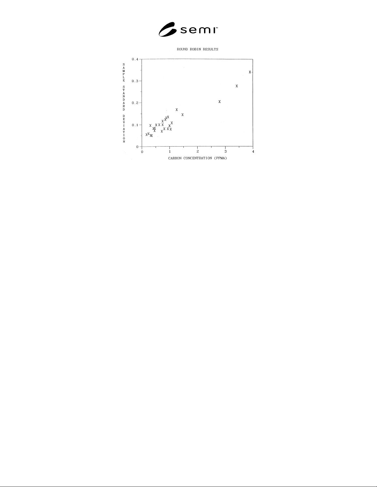
Figure 2
Round Robin Results
NOTICE: SEMI makes no warranties or representations as to the suitability of the standards set forth
herein for any particular application. The determination of the suitability of the standard is solely the
responsibility of the user. Users are cautioned to refer to manufacturer's instructions, product labels,
product data sheets, and other relevant literature, respecting any materials or equipment mentioned
herein. These standards are subject to change without notice.
By publication of this standard, Semiconductor Equipment and Materials International (SEMI) takes no
position respecting the validity of any patent rights or copyrights asserted in connection with any items
mentioned in this standard. Users of this standard are expressly advised that determination of any such
patent rights or copyrights, and the risk of infringement of such rights are entirely their own
responsibility.
Copyright by SEMI® (Semiconductor Equipment and Materials
International), 3081 Zanker Road, San Jose, CA 95134. Reproduction o
f
the contents in whole or in part is forbidden without express written
consent of SEMI.

SEMI MF1392-1103 © SEMI 2003 1
SEMI MF1392-1103
TEST METHOD FOR DETERMINING NET CARRIER DENSITY
PROFILES IN SILICON WAFERS BY CAPACITANCE-VOLTAGE
MEASUREMENTS WITH A MERCURY PROBE
This standard was technically approved by the Global Silicon Wafer Committee and is the direct
responsibility of the North American Silicon Wafer Committee. Current edition approved for publication by
the North American Regional Standards Committee on July 12, 2003. Initially available at www.semi.org
October 2003; to be published November 2003. Originally published by ASTM International as ASTM
F 1392-92. Last previous edition ASTM F 1392-02.
1 Purpose
1.1 Net carrier density is a critical parameter in growth
of epitaxial layers of silicon. This test method provides
a means for determining net carrier density without
formation of a special diode structure on the layer. It
may also be used in characterizing net carrier density in
polished silicon wafers.
1.2 This test method can be used for research and
development, process control, and materials specifi-
cation, evaluation, and acceptance purposes.
1.3 In the absence of interlaboratory test data to
establish its reproducibility (see Section 14.2), this test
method should be used for materials specification and
acceptance only after the parties to the test have
established reproducibility and correlation.
2 Scope
2.1 This test method
1
covers the measurement of net
carrier density and net carrier density profiles in
epitaxial and polished bulk silicon wafers in the range
from about 4 × 10
13
to about 8 × 10
16
carriers/cm
−3
(resistivity range from about 0.1 to about 100 Ω·cm in
n-type wafers and from about 0.24 to about 330 Ω·cm
in p-type wafers).
2.2 This test method requires the formation of a
Schottky barrier diode with a mercury probe contact to
an epitaxial or polished wafer surface. Chemical
treatment of the silicon surface may be required to
produce a reliable Schottky barrier diode.
2
The surface
treatment chemistries are different for n- and p-type
wafers. This test method is sometimes considered
destructive due to the possibility of contamination from
1 DIN 50439, Determination of the Dopant Concentration Profile of
a Single Crystal Semiconductor Material by Means of the
Capacitance-Voltage Method and Mercury Contact, is technically
equivalent to this test method. DIN 50439 is the responsibility of
DIN Committee NMP 221, with which SEMI maintains close liaison.
DIN 50439 is available in German and English from Beuth Verlag
GmbH, Burggrafenstraße 4-10, D-10772, Berlin, Germany.
2 Severin, P. J., and Poodt, G. J.,“Capacitance-Voltage
Measurements with a Mercury-Silicon Diode,” J. Electrochem. Soc,
119, 1384–1388 (1972).
the Schottky contact formed on the wafer surface;
however, repetitive measurements may be made on the
same test specimen.
2.3 This test method may be applied to epitaxial layers
on the same or opposite conductivity type substrate.
This test method includes descriptions of fixtures for
measuring substrates with or without an insulating
backseal layer.
2.4 The depth of the region that can be profiled
depends on the doping level in the test specimen.
Based on data reported by Severin
2
and Grove,
3
Figure
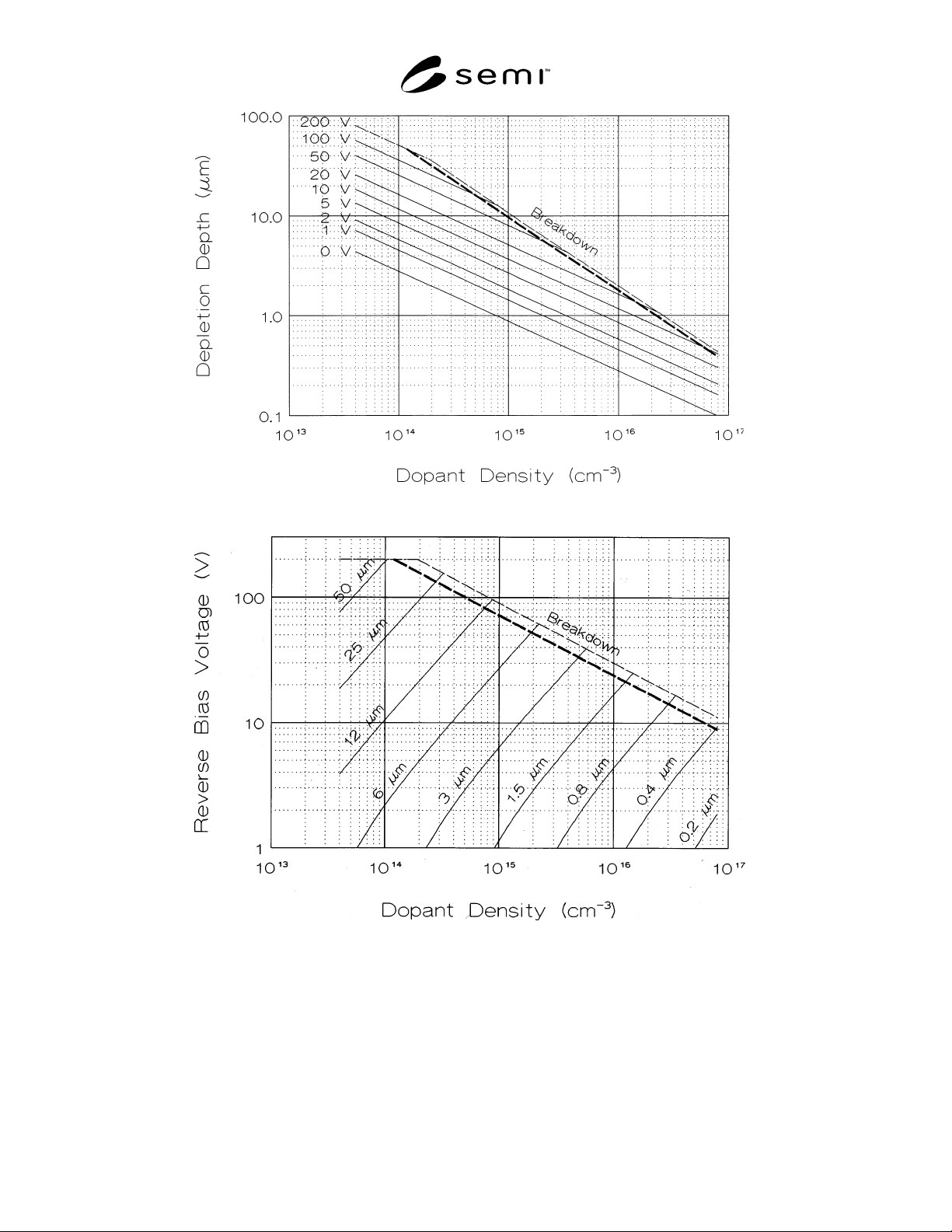
1 shows the relationships between depletion depth,
dopant density, and applied voltage together with the
breakdown voltage of a mercury silicon contact. The
test specimen can be profiled from approximately the
depletion depth corresponding to an applied voltage of
1 V to the depletion depth corresponding to the
maximum applied voltage (200 V or about 80% of the
breakdown voltage, whichever is lower). To be
measured by this test method, a layer must be thicker
than the depletion depth corresponding to an applied
voltage of 2 V.
2.5 This test method is intended for rapid carrier
density determination when extended sample
preparation time or high temperature processing of the
wafer is not practical.
2.6 This test method provides for determining the
effective area of the mercury probe contact using
polished bulk reference wafers that have been measured
for resistivity at 23° C in accordance with SEMI MF84
(see Note 1). This test method also includes procedures
for calibration of the apparatus for measuring both
capacitance and voltage.
NOTE 1: An alternative method of determining the effective
area of the mercury probe contact that involves the use of
reference wafers whose net carrier density has been measured
using fabricated mesa or planar p-n junction diodes or
evaporated Schottky diodes is not included in this test method
but may be used if agreed upon by the parties to the test.
3 Grove, A. S., Physics and Technology of Semiconductor Devices
(John Wiley and Sons, New York, 1967) Sections 6.2 and 6.7c.
SEMI MF1392-1103 © SEMI 2003 2
(a) Depletion Depth as a Function of Dopant Density with Applied Reverse Bias Voltage as a Parameter.
(b) Applied Reverse Bias Voltage as a Function of Dopant Density with Depletion as a Parameter.
Note: The light dashed line represents the applied reverse bias voltage at which breakdown occurs in a
mercury-silicon contact; the heavy dashed line represents 80 % of this voltage, it is recommended that the
applied reverse bias voltage not exceed this value. The light chain-dot line represents the maximum
reverse bias voltage specified in this test method.
Figure 1
Relationship Between Depletion Depth, Applied Reverse Bias Voltage, and Dopant Density