semi合集-English.pdf - 第7048页
SEMI S15-0200 © SEMI 2000 8 Perfor mance Manufacture r/Tec hnology Character istics A. B. C. D E. Reliability Replac ement/ Replenishm ent Resolution Respons e Time RFI/EMI Susceptibility Self-te st Sensor Ex change Sens…
SEMI S15-0200 © SEMI 20007
APPENDIX 1
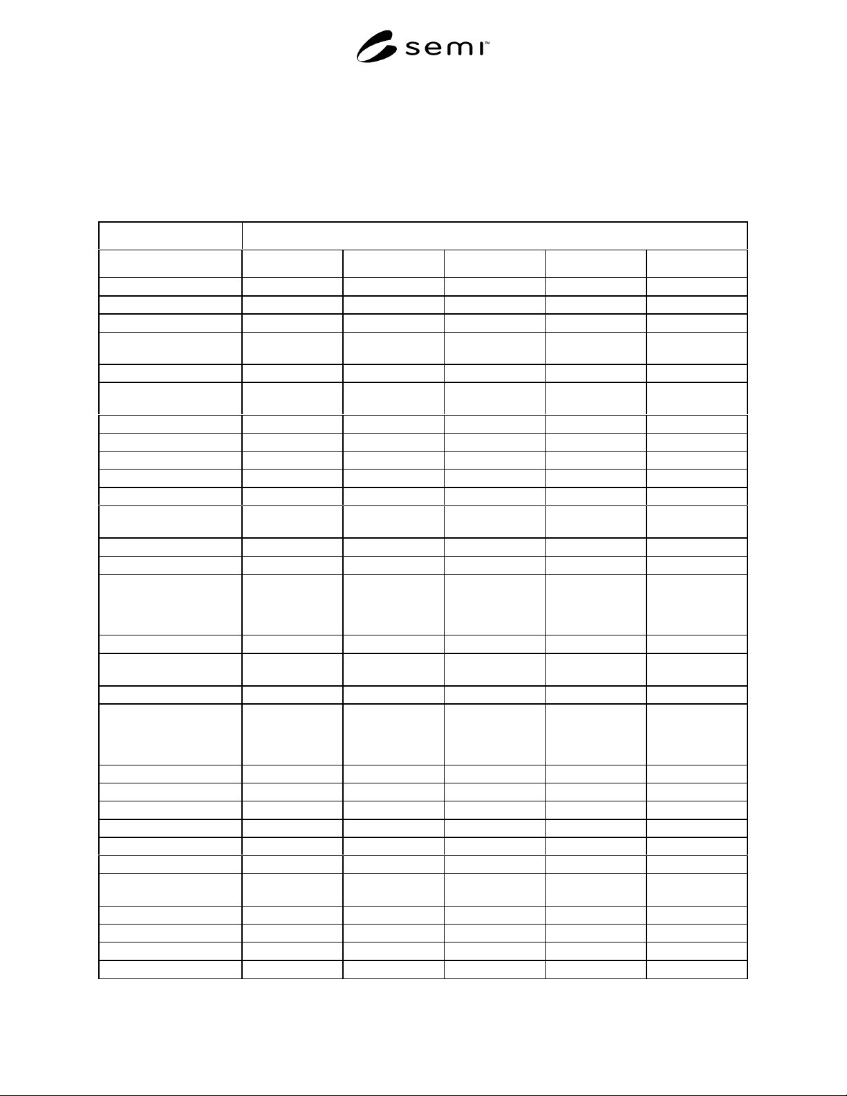
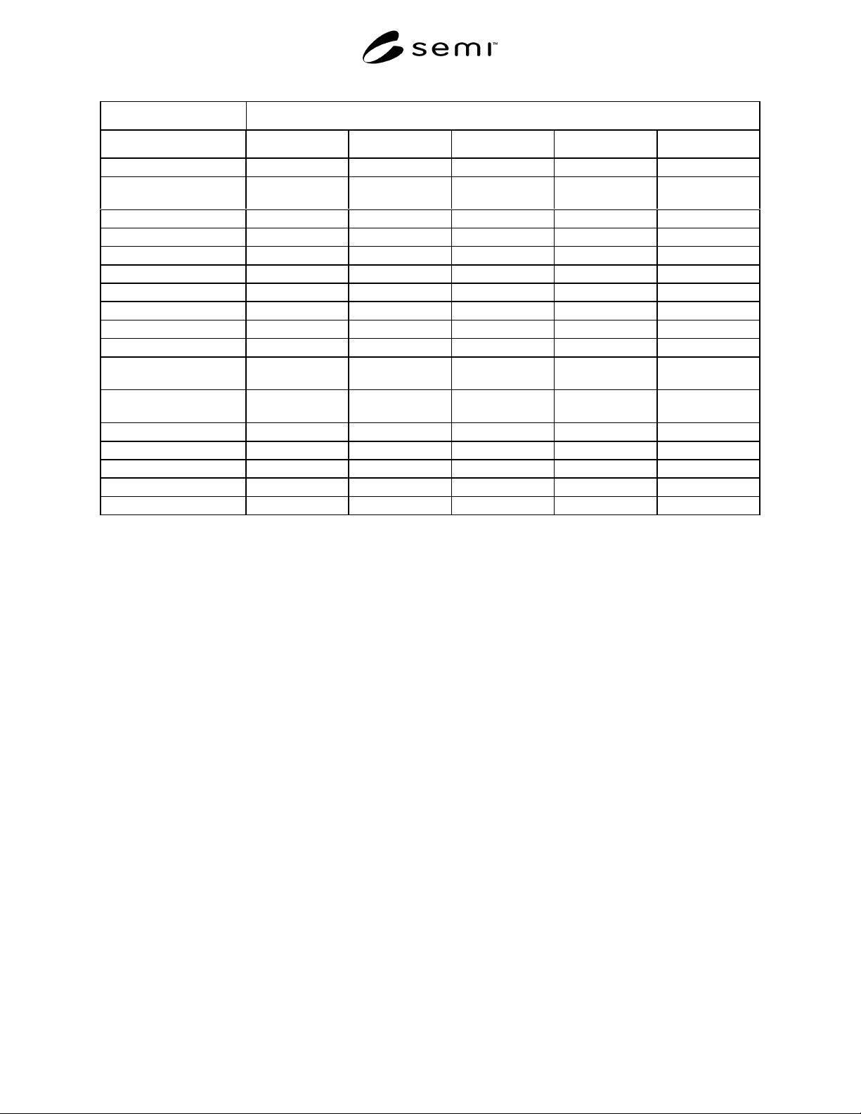
TABLE FOR COMPARISON OF PERFORMANCE CHARACTERISTICS
NOTE: The material in this appendix is an official part of SEMI S15 and was approved by full letter ballot procedures on
December 15, 1999 by the North American Regional Standards Committee.
Table A1-1
Performance Manufacturer/Technology
Characteristics A. B. C. D E.
Accuracy
Alarms
Calibration
Certifications and
Classifications
Communications (Serial)
Conditioning
Requirements
Cost of Ownership
Data Archiving
Diagnostics
Display
Drift
Environmental
Conditions
Equipment Failure
Expansion Flexibility
Extractive Systems:
Sampling Distance
Sample Cycle Time
Sample Contamination
Filter Lag
Installation (Wiring
Configuration)
Isolation
Limits of Detection:
Lowest Alarm Level
Limit of Detection
Upper limit of Detection
Linearity
Maintenance Interval
Other Utilities
Outputs
Physical Size
Poisoning
Position Effect
(Attitude Sensitivity)
Power Outage
Power Requirements
Recovery Time
Repeatability
SEMI S15-0200 © SEMI 2000 8
Performance Manufacturer/Technology
Characteristics A. B. C. D E.
Reliability
Replacement/
Replenishment
Resolution
Response Time
RFI/EMI Susceptibility
Self-test
Sensor Exchange
Sensor Specificity
Service and Support
Spare Parts Availability
Special Handling
Considerations
Storage and Shelf-life
Requirements
System Check
System Flexibility
Wake Up Requirements
Warm Up Period
Warranty
NOTICE: SEMI makes no warranties or representations as to the suitability of the guidelines set forth herein for
any particular application. The determination of the suitability of this guideline is solely the responsibility of the
user. Users are cautioned to refer to manufacturer’s instructions, product labels, product data sheets, and other
relevant literature respecting any materials mentioned herein. This guideline is subject to change without notice.
The user’s attention is called to the possibility that compliance with this guideline may require use of copyrighted
material or of an invention covered by patent rights. By publication of this guideline, SEMI takes no position
respecting the validity of any patent rights or copyrights asserted in connection with any item mentioned in this
guideline. Users of this guideline are expressly advised that determination of any such patent rights or copyrights,
and the risk of infringement of such rights, are entirely their own responsibility.
Copyright by SEMI® (Semiconductor Equipment and Materials
International), 3081 Zanker Road, San Jose, CA 95134. Reproduction o
f
the contents in whole or in part is forbidden without express written
consent of SEMI.

SEMI S16-0600 © SEMI 20001
SEMI S16-0600
ENVIRONMENTAL, HEALTH AND SAFETY GUIDELINES FOR
SEMICONDUCTOR MANUFACTURING EQUIPMENT DISPOSAL
These guidelines were technically approved by the Global Environmental, Health and Safety Committee and
are the direct responsibility of the Japanese Environmental, Health and Safety Committee. Current edition
approved by the Japanese Regional Standards Committee on April 28, 2000. Initially available on
www.semi.org June 2000; to be published June 2000.
1 Purpose
1.1 This document provides guidelines to minimize
hazards to workers and impacts to the environment
during equipment and component disposal.
2 Scope
2.1 These guidelines apply to the disposal of
semiconductor manufacturing equipment, its materials
and components and equipment design consideration to
facilitate disposal.
2.2 These guidelines are intended to be voluntary best
practices for this industry. These guidelines apply to
disposal parties, equipment designers, equipment
manufacturers, equipment suppliers and equipment
owners. The information should be provided to the
disposal party by the equipment owner prior to contract
negotiations.
2.3 These safety guidelines do not purport to address
all of the safety issues associated with its use. It is the
responsibility of the users of these guidelines to
establish appropriate safety and health practices and
determine the applicability of regulatory limitations
prior to use.
3 Limitation
3.1 These guidelines are not intended to supersede the
applicable codes and regulations of the region where
the equipment is disposed.
3.2 Section 6 in these guidelines should be applied not
to existing models and subsystems but to newly
designed models and subsystems after publication of
these guidelines.
4 Referenced Standards
4.1 SEMI Standards
SEMI S1 Safety Guidelines for Visual Hazard Alerts
SEMI S2 Environmental, Health, and Safety
Guideline for Semiconductor Manufacturing Equipment
SEMI S10 Safety Guideline for Risk Assessment
SEMI S12 Environment, Health and Safety
Guidelines for Equipment Decontamination
SEMI S13 Safety Guidelines for Operation and
Maintenance Manuals Used with Semiconductor
Manufacturing Equipment
4.2 ISO Documents
1
ISO11469 Plastics; Generic Identification and
Marking of Plastic Products
ISO14001 1996 Environment Management Systems,
Specifications with Guideline for Use
4.3 CEN
2
/ CENELEC
3
Document
EN1050 Safety of Machinery—Principles for Risk
Assessment
4.4 OSHA Document
4
29 CFR 1910. 1200 Labor
NOTE 1: As listed or revised, all documents cited shall be the
latest publications of adopted standards.
5 Terminology
5.1 Terminology defined in SEMI S1, S2, S12, and
S13 should be referred to except if otherwise specified
below.
5.1.1 decontaminate
to remove all known hazards
from equipment, including chemical, physical,
electrical, to a level that will not pose a threat or harm
to humans or the environment. This level may be set by
each country, state and local regulations or industry
practice.
5.1.2 decontamination
the process required to
remove hazards to an acceptable level of risk (see
Section 5.1).
1 International Standards Organization, 1, rue de Varembe, Case
postale 56, CH-1211 Geneve 20, Switzerland.
2 European Committee for Standardization, 36, rue de Stassart, B-
1050 Brussels, Belgium
3 European Committee for Electrotechnical Standardization, Rue de
Stassart, 35, B-1050 Brussels, Belgium
4 US Government Printing Office, Washington, D.C. 20402