semi合集-English.pdf - 第6024页
SEMI G2-94 © SEMI 1 994 4 Table 1 Ty pical Ceramic Cer-DIP Metallic Leadframe s Dimension and Tolerance Re quirements Desc ription Cavity Length Cavity W idth Lead-For med Widt h, Top Bond Finge r Layout End vs. Side Nom…

SEMI G2-94 © SEMI 19943
9 Test Methods
9.1 Sequence of Events and Tests
The sequence of testing should be:
9.1.1 Degrease
9.1.2 Metallurgical Bond Adhesion (Section 9.3.1)
9.1.3 Frame Attach
9.1.4 Die Attach
9.1.5 Bond
9.1.6 Pre-Seal Bond Pull (Section 9.3.2)
9.1.7 Seal
9.1.8 Mechanical Testing (Section 9.2)
9.1.9 Lead Trim
9.1.10 Post-Seal Bond Pull (Section 9.3.2)
NOTE: It is acknowledged that the leadframe manufacturer
may not perform all these tests due to equipment and
component limitations. Regardless, leadframes must fulfill
these requirements, subject to the influence of the testing
facility and associated components.
9.2 Mechanical and Thermal
9.2.1 Temperature Cycling — Per MIL-STD-883,
Method 1010.4, Condition C.
9.2.2 Thermal Shock — Per MIL-STD-883, Method
1011.2, Condition C.
9.2.3 Centrifuge — Per MIL-STD-883, Method
2001.2, Condition E.
9.2.4 Lead Integrity
9.2.4.1 A 500°C ± 20° - 55% R.H. heat soak for 15
minutes ± 1 minute. Cooled at no more than 50°C per
minute. Afterwards the frame is clamped between
plates of a suitable size for the lead spacing (see Section
9.2.4.2). Then (3) 90° cycles are performed. Frames are
examined at 20× magnification and if cracks are
observed at the Apex A (Figure 3), then the frame is
rejected.
9.2.4.2 Plate shall be of equivalent plan-form to the
ceramic being employed for the particular frame. An
edge radius equivalent to 2T, where T is the leadframe
thickness, shall be on the contacting surface of the
plate.
9.3 Functional Test Methods
9.3.1 Metallurgical Bond Adhesion Aluminization —
The metallurgical bond between the aluminization and
the base metal shall permit the leadframe to be heated
in air to 525°C ± 10°C for five (5) minutes minimum
without evidence of aluminum peeling, blistering, or
discoloring when viewed at 20× magnification. (Dis-
coloration must not jeopardize the user’s standard part
reliability.) Subsequently, the aluminized layer must
pass the following two adhesion tests:
9.3.1.1 A cellophane type adhesive tape is firmly
applied to the aluminization and removed toward the
center of the cavity in a continuous rapid motion. This
test is to be performed over the same area three times.
No evidence of aluminum separation from the base
metal shall be visible at 20× magnification
9.3.1.2 The aluminization shall be capable of passing a
functional wirebond test without separating.
9.3.2 Lead Bond Quality — Minimum pre-seal and
post-seal bond strength test per MIL-STD-883, Method
2011.2, Test Condition D. Applicable failure
categories: A-4 and A-6.
10 Packaging and Marking
10.1 Packaging — The shipping containers and
materials shall be suitably designed to provide the
singulated components with protection against normal
transportation damage risks which include crushing,
abrasion and spillage, and exposure to moisture and
other corrosive gases. The inner packing materials must
not cause particulate contamination on the components
and shall be clean-room compatible as defined by the
customer. The components, in packing trays, shall be
sealed in a vacuum bag with a dessicant.
10.2 Packing List
10.2.1 Internal Packages — Each internal package
shall be marked as follows:
User Part Number
User Purchase Order Number
Drawing Number (User’s and Supplier’s, if
appropriate)
Supplier Shipping Lot Number
Quantity
Date of Manufacture
10.2.2 External Packages — The Packing List, located
on the outside of the container, shall provide the
following information:
User’s Part Number
User’s Purchase Order Number
Quantity
Shipping Date
Any specific instructions for receiving dock
personnel.
SEMI G2-94 © SEMI 1994 4
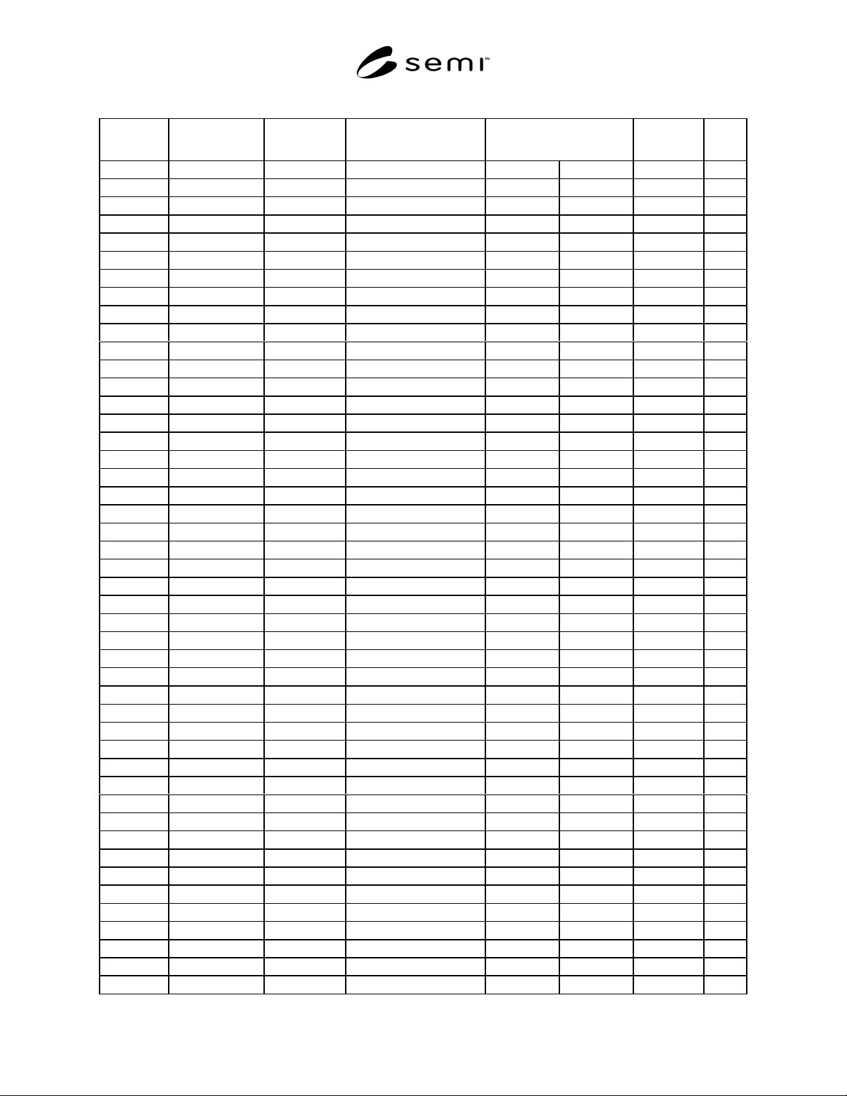
Table 1 Typical Ceramic Cer-DIP Metallic Leadframes Dimension and Tolerance Requirements
Description Cavity Length Cavity Width Lead-Formed Width, Top
Bond Finger Layout
End vs. Side
Nominal
Progression Unit
8SSI - 0.120 ± 0.007 0.311 ± 0.003 0 4 0.945 in
3.05 ± 0.178 7.90 ± 0.076 24.00 mm
8MSI - 0.140 ± 0.007 0.311 ± 0.003 0 4 0.945 in
3.56 ± 0.178 7.90 ± 0.076 24.00 mm
8LSI - 0.160 ± 0.007 0.311 ± 0.003 0 4 0.945 in
4.06 ± 0.178 7.90 ± 0.076 24.00 mm
14SSI 0.160 ± 0.007 0.120 ± 0.007 0.311 ± 0.003 4 3 0.945 in
4.06 ± 0.178 3.05 ± 0.178 7.90 ± 0.076 24.00 mm
14MSI 0.260 ± 0.007 0.140 ± 0.007 0.311 ± 0.003 4 3 0.945 in
6.60 ± 0.178 3.56 ± 0.178 7.90 ± 0.076 24.00 mm
16SSI 0.160 ± 0.007 0.120 ± 0.007 0.311 ± 0.003 4 4 0.945 in
4.06 ± 0.178 3.05 ± 0.178 7.90 ± 0.076 24.00 mm
16MSI 0.260 ± 0.007 0.140 ± 0.007 0.311 ± 0.003 4 4 0.945 in
6.60 ± 0.178 3.56 ± 0.178 7.90 ± 0.076 24.00 mm
16LSI 0.260 ± 0.007 0.170 ± 0.007 0.311 ± 0.003 4 4 0.945 in
6.60 ± 0.178 4.32 ± 0.178 7.90 ± 0.076 24.00 mm
16SLSI 0.360 ± 0.007 0.170 ± 0.007 0.311 ± 0.003 4 4 0.945 in
9.14 ± 0.178 4.32 ± 0.178 7.90 ± 0.076 24.00 mm
16VLSI 0.330 ± 0.007 0.180 ± 0.007 0.311 ± 0.003 6 2 0.945 in
8.38 ± 0.178 4.57 ± 0.178 7.90 ± 0.076 24.00 mm
18MSI 0.260 ± 0.008 0.140 ± 0.008 0.311 ± 0.003 4 5 1.061 in
6.60 ± 0.203 3.56 ± 0.203 7.90 ± 0.076 26.95 mm
18LSI 0.260 ± 0.008 0.170 ± 0.008 0.311 ± 0.003 6 3 1.061 in
6.60 ± 0.203 4.32 ± 0.203 7.90 ± 0.076 26.95 mm
18VLSI 0.330 ± 0.008 0.180 ± 0.008 0.311 ± 0.003 6 3 1.061 in
8.38 ± 0.203 4.57 ± 0.203 7.90 ± 0.076 26.95 mm
20MSI 0.210 ± 0.008 0.140 ± 0.008 0.311 ± 0.003 4 6 1.175 in
5.33 ± 0.203 3.56 ± 0.203 7.90 ± 0.076 29.85 mm
20LSI 0.260 ± 0.008 0.170 ± 0.008 0.311 ± 0.003 6 4 1.175 in
6.60 ± 0.203 4.32 ± 0.203 7.90 ± 0.076 29.85 mm
20VLSI 0.330 ± 0.008 0.175 ± 0.008 0.311 ± 0.003 6 4 1.175 in
8.38 ± 0.203 4.45 ± 0.203 7.90 ± 0.076 29.85 mm
22MSI 0.270 ± 0.010 2.10 ± 0.010 0.411 ± 0.003 6 5 1.250 in
6.86 ± 0.254 5.33 ± 0.254 10.44 ± 0.076 31.75 mm
22LSI 0.310 ± 0.010 0.240 ± 0.010 0.411 ± 0.003 6 5 1.250 in
7.87 ± 0.254 6.10 ± 0.254 10.44 ± 0.076 31.75 mm
22VLSI 0.350 ± 0.010 0.260 ± 0.010 0.411 ± 0.003 8 3 1.250 in
8.89 ± 0.254 6.60 ± 0.254 10.44 ± 0.076 31.75 mm
24MSI 0.260 ± 0.010 0.260 ± 0.010 0.611 ± 0.003 6 6 1.510 in
8.38 ± 0.254 6.60 ± 0.254 15.01 ± 0.076 38.35 mm
24LSI 0.330 ± 0.010 0.285 ± 0.010 0.611 ± 0.003 6 6 1.510 in
8.38 ± 0.254 7.24 ± 0.254 15.01 ± 0.076 38.35 mm
24VLSI 0.420 ± 0.010 0.290 ± 0.010 0.611 ± 0.003 6 6 1.510 in
10.67 ± 0.254 7.37 ± 0.254 15.01 ± 0.076 38.35 mm
24SD3S 0.260 ± 0.010 0.170 ± 0.010 0.311 ± 0.003 6 6 1.510 in
6.60 ± 0.254 4.32 ± 0.254 7.90 ± 0.076 38.35 mm
SEMI G2-94 © SEMI 19945
Description Cavity Length Cavity Width Lead-Formed Width, Top
Bond Finger Layout
End vs. Side
Nominal
Progression Unit
24SD3M 0.430 ± 0.010 0.180 ± 0.010 0.311 ± 0.003 8 4 1.510 in
10.92 ± 0.254 4.57 ± 0.254 7.90 ± 0.076 38.35 mm
24SD4M 0.210 ± 0.010 0.210 ± 0.010 0.411 ± 0.003 6 6 1.510 in
5.33 ± 0.254 5.33 ± 0.254 10.44 ± 0.076 38.35 mm
28MSI 0.260 ± 0.011 0.260 ± 0.011 0.611 ± 0.003 8 6 1.724 in
6.60 ± 0.279 6.60 ± 0.279 15.01 ± 0.076 43.79 mm
28LSI 0.325 ± 0.011 0.275 ± 0.011 0.611 ± 0.003 8 6 1.724 in
8.26 ± 0.279 6.99 ± 0.279 15.01 ± 0.076 43.79 mm
28VLSI 0.420 ± 0.011 0.280 ± 0.011 0.611 ± 0.003 8 6 1.724 in
10.67 ± 0.279 7.11 ± 0.279 15.01 ± 0.076 43.79 mm
40MSI 0.270 ± 0.012 0.260 ± 0.012 0.611 ± 0.003 10 10 2.300 in
6.86 ± 0.305 6.60 ± 0.305 15.01 ± 0.076 58.42 mm
40LSI 0.375 ± 0.012 0.295 ± 0.012 0.611 ± 0.003 12 8 2.300 in
9.53 ± 0.305 7.49 ± 0.305 15.01 ± 0.076 58.42 mm
NOTE: While a 0.311 top form is still currently being used, numerous users have changed to a 0.314 top form to prevent interference between the
Cer-DIP base and leadframe.
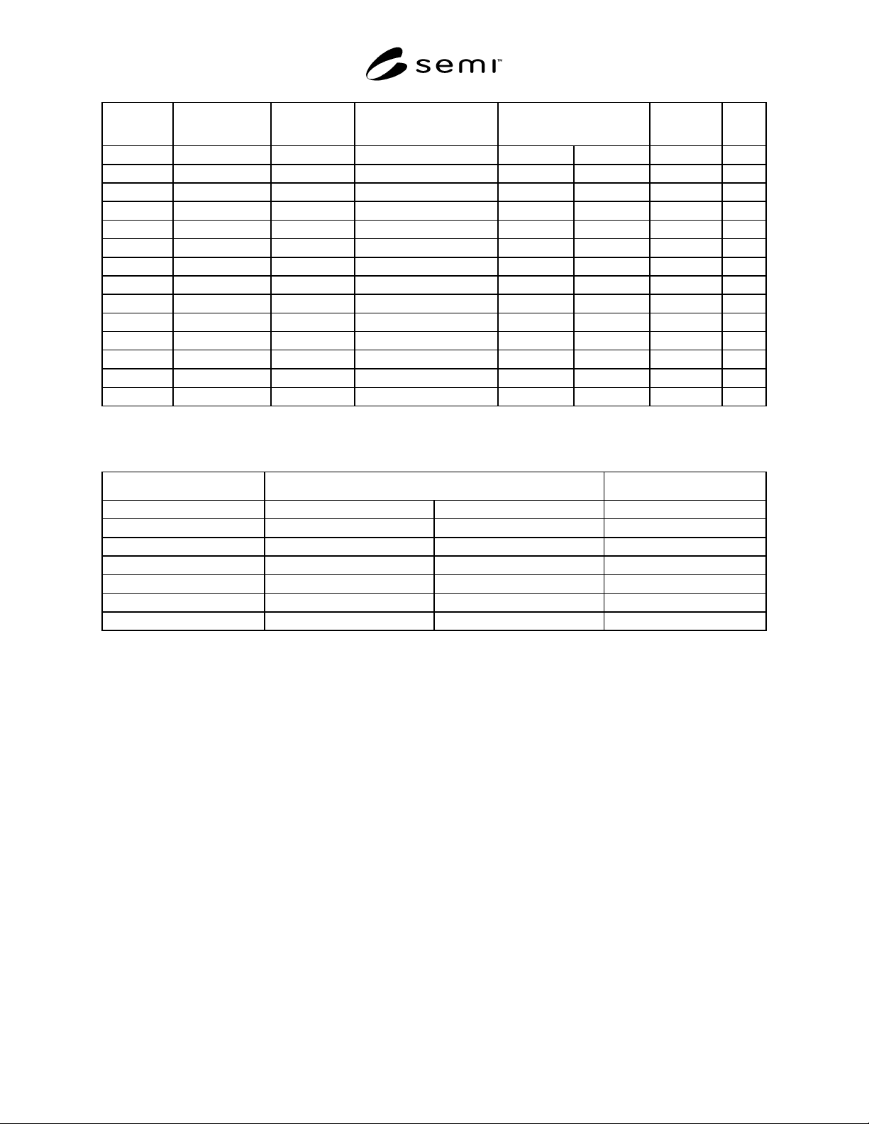
Table 2
Leads Planarity Coplanarity
8–14–16 +0.003"/–0.004" (+ 0.076 mm/–0.102 mm) 0.004" (0.102 mm)
18 +0.004"/–0.005" (+0.102 mm/–0.127 mm) 0.005" (0.127 mm)
20 +0.004"/–0.005" (+0.102 mm/–0.127 mm) 0.006" (0.152 mm)
22 +0.004"/–0.006" (+0.102 mm/–0.152 mm) 0.006" (0.152 mm)
24 +0.004"/–0.006" (+0.102 mm/–0.152 mm) 0.007" (0.178 mm)
28 +0.005"/–0.007" (+0.127 mm/–0.178 mm) 0.008" (0.203 mm )
40 +0.006"/–0.008" (+0.152 mm/–0.203 mm) 0.010" (0.254 mm)