semi合集-English.pdf - 第4895页
SEMI M4-1103 © SEMI 1978, 2003 5 9 Certification 9.1 Upon re quest of the purchaser in the cont ract or order, a manufact urer’s or suppl ier’s certifi cation that the material was manufacture d and tested in accordance …
SEMI M4-1103 © SEMI 1978, 2003 4
7.2.7 Surface Defects and Contamination — Determine
by methods agreed upon between user and supplier.
SEMI MF154 is a useful guide for defining a variety of
surface features and establishing commonly understood
terms for describing surface defects and contamination.
SEMI MF523 is also recommended (see Note 5).
Recommended maximum levels of surface defects and
contamination are listed in Table 2.
NOTE 4: SOS wafers are susceptible to surface damage. The
thin film on the hard sapphire substrate may be damaged
physically in ways that are not immediately evident. Special
care must therefore be used in the selection and execution of
measurement procedures.
NOTE 5: In SEMI MF523, defects commonly found in
silicon wafers are defined. Some of these terms do not apply
to SOS wafers, but are included in Table 2 to provide a
convenient reference point to the silicon wafer and epitaxial
wafer standards. In this case, the recommended maximum
acceptable limit is shown as N.A. (not applicable).
8 Sampling
8.1 Unless otherwise specified, ASTM Practice E 122
shall be used. When so specified, appropriate sample
sizes shall be selected from each lot according to
ANSI/ASQC Z1.4-1993. Each quality characteristic
shall be assigned an acceptable quality level (AQL) and
lot total percent defective (LTPD) value in accordance
with ANSI/ASQC Z1.4-1993 definitions for critical,
major, and minor classifications. If desired and so
specified in the contract or order, each of these
classifications may alternatively be assigned cumulative
AQL and LTPD values. Inspection levels shall be
agreed upon between user and supplier.
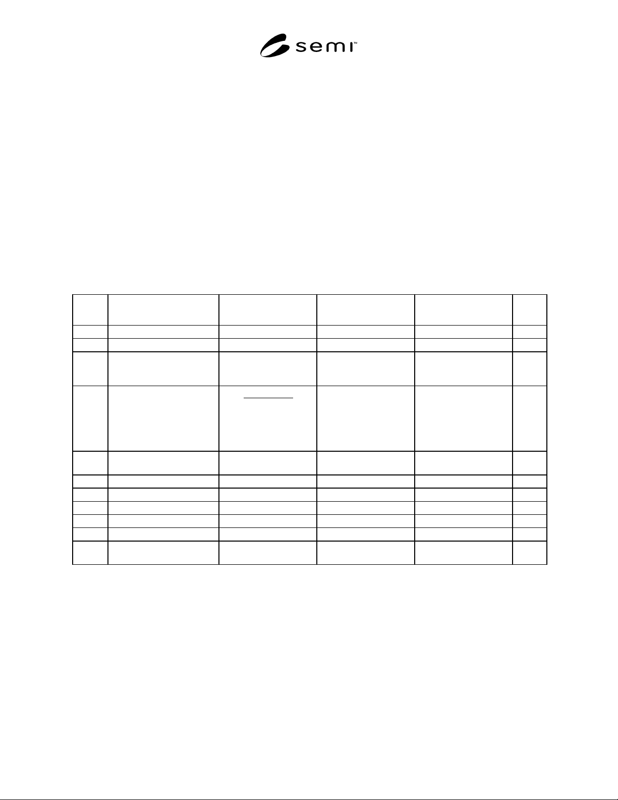
Table 2 Recommended Maximum Surface Defects Levels by Non-Destructive Means
ITEM
CHARACTERISTICS
MAX ACCEPTABLE
LIMIT
TEST METHOD
DEFECT DEFINITION
PER
NOTES
1 STACKING FAULTS N.A. 2
2 SLIP N.A. 2
3 PROTRUDING DEFECTS
(Including spikes, hillocks,
pyramids, and inclusions)
N.A. 2
4 PITS Diameter No.
2" 4
3" 9
100 mm 15
125 mm 20
150 mm 25
SEMI MF523 SEMI MF154 1, 3
5 SCRATCHES Cumulative L
1/2 wafer radius
SEMI MF523 SEMI MF154 1, 3
6 CRACKS, FRACTURES None SEMI MF523 SEMI MF154 5
7 ORANGE PEEL N.A. 2
8 EDGE CHIPS Max No. 2 SEMI MF523 SEMI MF154 2
9 EDGE CROWN N.A. 2
10 HAZE None SEMI MF523 SEMI MF154 1, 6
11 FOREIGN MATTER
FINGER PRINTS
None SEMI MF523 SEMI MF154 1, 7
NOTE 1: The outer 4 mm annulus is excluded from these criteria.
NOTE 2: These defects are not observed in SOS wafers. Terms remain for convenient reference to epitaxial silicon wafer specification.
NOTE 3: Ninety percent of the wafers shall be free of these defects. Balance of wafer may have defects at these limits.
NOTE 4: All chips shall be beveled. Maximum penetration 3 mm. Pointed apex chips none. Chips less than 0.4 mm (0.015 in.) shall not be
counted. See SEMI M3, Table R1-1.
NOTE 5: Cracks are observed in sapphire as fractures or as surface separations along cleavage planes.
NOTE 6: Haze refers to the presence of polycrystalline silicon deposits in the film, as described in Section 7.2.5. Haze shall not be visible under
lighting conditions of ASTM F 523.
NOTE 7: Particulate matter easily removed by industry-accepted cleaning techniques shall not constitute foreign matter.

SEMI M4-1103 © SEMI 1978, 2003 5
9 Certification
9.1 Upon request of the purchaser in the contract or
order, a manufacturer’s or supplier’s certification that
the material was manufactured and tested in accordance
with this specification, together with a report of the test
results, shall be furnished at the time of shipment.
9.2 In the interest of controlling inspection costs, the
supplier and purchaser may agree that the material shall
be certified as “capable of meeting” certain
requirements. In this context, “capable of meeting”
shall signify that the supplier is not required to perform
the appropriate tests in Section 7; however, if the
purchaser performs the test and the material fails to
meet the requirements, the material may be subject to
rejection.
10 Packing and Marking
10.1 Special packing requirements shall be subject to
agreement between the user and supplier. Otherwise all
wafers shall be handled, inspected, and packed in such
a manner as to avoid chipping, scratches, and
contamination, and in accordance with the best industry
practices to provide protection against damage during
shipment.
10.2 The wafers supplied under these specifications
shall be identified by appropriately labeling the outside
of each box or container, and each subdivision thereof,
in which it may reasonably be expected that the wafers
will be stored prior to further processing. Identification
shall include supplier’s name and reference number,
purchaser’s part number, purchaser order number,
quantity, dopant, conductivity type of epitaxial layers,
resistivity and thickness of the epitaxial layer; the
reference number assigned by the supplier shall provide
ready access to information concerning the fabrication
history of the particular substrates in that lot. Such
information shall be retained on file at the
manufacturer’s facility for at least one month after that
particular lot has been accepted by the purchaser.
NOTICE: SEMI makes no warranties or
representations as to the suitability of the standards set
forth herein for any particular application. The
determination of the suitability of the standard is solely
the responsibility of the user. Users are cautioned to
refer to manufacturer’s instructions, product labels,
product data sheets, and other relevant literature
respecting any materials mentioned herein. These
standards are subject to change without notice.
The user’s attention is called to the possibility that
compliance with this standard may require use of
copyrighted material or of an invention covered by
patent rights. By publication of this standard, SEMI
takes no position respecting the validity of any patent
rights or copyrights asserted in connection with any
item mentioned in this standard. Users of this standard
are expressly advised that determination of any such
patent rights or copyrights, and the risk of infringement
of such rights, are entirely their own responsibility.
Copyright by SEMI® (Semiconductor Equipment and Materials
International), 3081 Zanker Road, San Jose, CA 95134. Reproduction o
f
the contents in whole or in part is forbidden without express written
consent of SEMI.

SEMI M6-1000 © SEMI 1981, 20001
SEMI M6-1000
SPECIFICATION FOR SILICON WAFERS FOR USE AS
PHOTOVOLTAIC SOLAR CELLS
This specification was technically approved by the Global Silicon Wafer Committee and is the direct
responsibility of the European Materials Committee. Current edition approved by the European Regional
Standards Committee on July 28, 2000. Initially available at www.semi.org September 2000; to be published
October 2000. Originally published in 1981; previously published in 1985.
NOTE: This document replaces the previous version of SEMI M6 and M6.1, M6.2, M6.3, M6.4, and M6.5 in
their entirety.
1 Purpose
1.1 This specification covers the r equirements for
silicon wafers for use in photovoltaic (PV) solar cell
manufacture.
2 Scope
2.1 The dimensional characteristic s, crystalline defects
and commonly used wafer electronic properties are
described. Two classes of crystalline silicon materials
are recognized: monocrystalline and multicrystalline.
2.2 This standard does not purport to address safety
issues, if any, associated with its use. It is the
responsibility of the users of this standard to establish
appropriate safety and health practices and determine
the applicability of regulatory limitations prior to use.
2.3 SI (System International) units are used
throughout.
3 Referenced Standards
NOTE 1: The specification recognizes only two discrete
material forms monocrystalline and multicrystalline. In the
monocrystalline form one crystallographic orientation
describes the whole wafer and in the multicrystalline case
there is more than one crystallographic orientation present.
3.1 SEMI Standard
SEMI M1 — Specifications for Polished
Monocrystalline Silicon Wafers
3.2 ASTM Standards
1
E 122 — Standard Practice for Choice of Sample Size
to Estimate the Average for a Characteristic of a Lot or
Process
F 26 — Standard Test Methods for Determining the
Orientation of a Semiconductive Single Crystal
F 28 — Standard Test Methods for Minority-Carrier
Lifetime in Bulk Germanium and Silicon by
Measurement of Photoconductivity Decay
1 American Society for Testing and Materials, 100 Barr Harbor
Drive, West Conshohocken, PA 19428-2959
F 42 — Standard Test Methods for Conductivity Type
of Extrinsic Semiconducting Materials
F 43 — Standard Test Methods for Resistivity of
Semiconductor Materials
F 84 — Standard Test Method for Measuring
Resistivity of Silicon Wafers with an In-Line Four-
Point Probe
F 391 — Standard Test Methods for Minority Carrier
Diffusion Length in Extrinsic Semiconductors by
Measurement of Steady-State Surface Photovoltage
F 398 — Standard Test Method for Majority Carrier
Concentration in Semiconductors by Measurement of
Wavenumber or Wavelength of the Plasma Resonance
Minimum
F 533 — Standard Test method for Thickness and
Thickness Variation of Silicon Wafers
F 613 — Standard Test Method for Measuring
Diameter of Semiconductor Wafers
F 657 — Standard Test Method for Measuring Warp
and Total Thickness Variation on Silicon Wafers by
Noncontact Scanning
F 673 — Standard Test Methods for Measuring
Resistivity of Semiconductor Slices or Sheet Resistance
of Semiconductor Films with a Noncontact Eddy-
Current Gage
F 1188 — Standard Test Method for Interstitial Atomic
Oxygen Content of Silicon by Infrared Absorption
F 1391 — Standard Test Method for Substitutional
Atomic Carbon Content of Silicon by Infrared
Absorption
F 1535 — Standard Test Method for Carrier
Recombination Lifetime in Silicon Wafers by
Noncontact Measurement of Photoconductivity Decay
by Microwave Reflectance
F 1619 — Standard Test Method for Measurement of
Interstitial Oxygen Content of Silicon Wafers by
Infrared Absorption Spectroscopy with p-Polarized
Radiation Incident at the Brewster Angle