semi合集-English.pdf - 第438页
SEMI E62-0705 © SEMI 1997, 2005 7 Symbol Used Value Specified Datum Measured from Feature Measured to z 32 84.5 mm (3.33 in.) maximum for 13-wafer cassette and 144.5 mm (5.69 in.) maximum for 25-wafer cassette z 30 above…
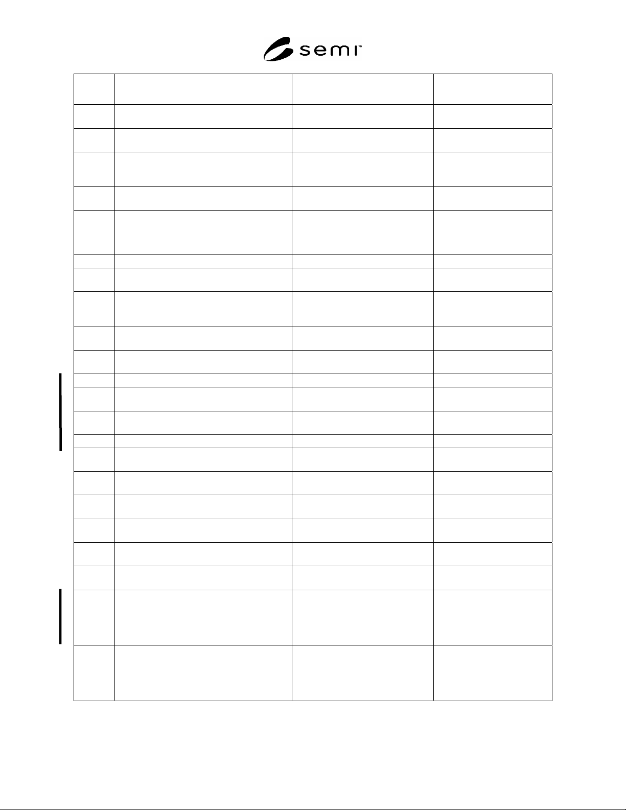
SEMI E62-0705 © SEMI 1997, 2005 6
Symbol
Used
Value Specified Datum Measured from Feature Measured to
r35 30 mm (1.18 in.) maximum not applicable outside corner of frame seal
zone
r36 6.75 ± 0.1 mm
(0.266 ± 0.004 in.)
intersection of x30 and z30 ends of latch key head
r38 27.5 mm (1.08 in.) minimum intersection of x31 and z31 boundary of vacuum
application zone around
registration pin
r40 0.4 ± 0.1 mm
(0.016 ± 0.004 in.)
not applicable blend at intersection of r30
with r31 and y32
r41 1.5 ± 0.2 mm
(0.059 ± 0.008 in.)
not applicable
b
lend at convex features on the
outer edge of the latch keys
(adjacent to the surface defined
by y36)
r45 1 mm (0.04 in.) maximum not applicable all concave features (radius)
r46 2 mm (0.08 in.) maximum not applicable all required convex features
(radius)
r47
0.80 m (32 in.)
maximum Roughness (R
a
)
as defined in ISO 4287
not applicable surface finish of the
registration pins and latch keys
x30 129 ± 0.1 mm
(5.08 ± 0.004 in.)
bilateral datum plane center line of latch key rotation
x31 70 ± 0.1 mm
(2.756 ± 0.004 in.)
bilateral datum plane center of registration pins
x32 173.5 mm (6.83 in.) maximum bilateral datum plane inside edge of door seal zone
x33 182.5 ± 0.25 mm
(7.185 ± 0.010 in.)
bilateral datum plane outside edge of door seal zone
x34 184.5 ± 0.25 mm
(7.264 ± 0.010 in.)
bilateral datum plane inside edge of frame seal zone
x35 193.5 mm (7.62 in.) minimum bilateral datum plane outside edge of frame seal zone
x36 2.5 ± 0.1 mm
(0.098 ± 0.004 in.)
x30 from bilateral datum plane side of latch key head
x37 ± 0.2 mm
(± 0.008 in.)
position of the load port door before
opening
position of the load port door
after closing
y31 7.5 mm (0.30 in.) point on door seal zone closest to
facial datum plane
origin of r30 (shoulder radius)
on registration pin
y32 11.0 ± 0.1 mm
(0.43 ± 0.004 in.)
point on door seal zone closest to
facial datum plane
end of registration pin
y36 7.0 ± 0.1 mm
(0.28 ± 0.004 in.)
point on door seal zone closest to
facial datum plane
far side of latch key head
y37 3.5 ± 0.1 mm
(0.14 ± 0.004 in.)
point on door seal zone closest to
facial datum plane
near side of latch key head
z30 106.5 ± 0 mm (4.19 ± 0 in.)
for 13-wafer cassette
and
166.5 ± 0 mm (6.56 ± 0 in.)
for 25-wafer cassette
horizontal datum plane vertical center line of port and
center line of latch key rotation
z31 45 ± 0.1 mm (1.772 ± 0.004 in.)
for 13-wafer cassette
and
105 ± 0.1 mm (4.134 ± 0.004 in.)
for 25-wafer cassette
z30 above horizontal datum plane center of registration pins
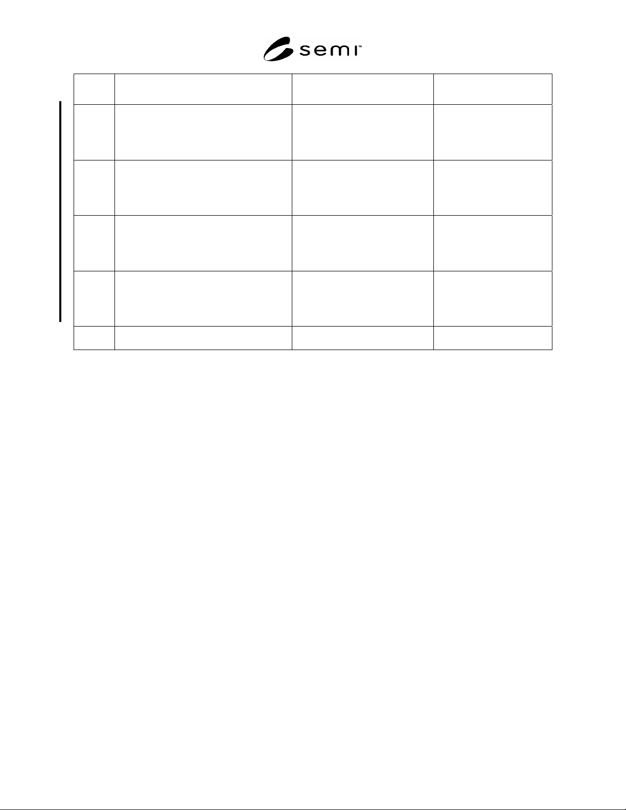
SEMI E62-0705 © SEMI 1997, 2005 7
Symbol
Used
Value Specified Datum Measured from Feature Measured to
z32 84.5 mm (3.33 in.) maximum
for 13-wafer cassette
and
144.5 mm (5.69 in.) maximum
for 25-wafer cassette
z30 above horizontal datum plane inside edge of door seal zone
z33 93.5 ± 0.25 mm (3.681 ± 0.010 in.)
for 13-wafer cassette
and
153.5 ± 0.25 mm (6.043 ± 0.010 in.)
for 25-wafer cassette
z30 above horizontal datum plane outside edge of door seal zone
z34 95.5 ± 0.25 mm (3.760 ± 0.010 in.)
for 13-wafer cassette
and
155.5 ± 0.25 mm (6.122 ± 0.010 in.)
for 25-wafer cassette
z30 above horizontal datum plane inside edge of frame seal zone
z35 104.5 mm (4.11 in.) minimum
for 13-wafer cassette
and
164.5 mm (6.48 in.) minimum
for 25-wafer cassette
z30 above horizontal datum plane outside edge of frame seal
zone
z37 ± 0.2 mm
(± 0.008 in.)
position of the load port door before
opening
position of the load port door
after closing
SEMI E62-0705 © SEMI 1997, 2005 8
APPENDIX 1
APPLICATION NOTES
NOTICE: This appendix was approved as an official part of SEMI E62, but the recommendations in this appendix are optional
and are not required to conform to this standard.
A1-1 Perpendicularity and parallelism are implicitly defined in the geometric tolerances.
A1-2 ¶6.1 discusses the need for clearance between the box and the tool’s front-opening interface when the box is
placed on the load port. After the box is placed on the load port, the kinematic couplings will move the box forward
to engage with the tool’s front-opening interface. The possibility of human fingers being pinched between the box
and the tool's front-opening interface may be a safety concern for tool designers.
NOTICE: SEMI makes no warranties or representations as to the suitability of the standards set forth herein for any
particular application. The determination of the suitability of the standard is solely the responsibility of the user.
Users are cautioned to refer to manufacturer's instructions, product labels, product data sheets, and other relevant
literature, respecting any materials or equipment mentioned herein. These standards are subject to change without
notice.
By publication of this standard, Semiconductor Equipment and Materials International (SEMI) takes no position
respecting the validity of any patent rights or copyrights asserted in connection with any items mentioned in this
standard. Users of this standard are expressly advised that determination of any such patent rights or copyrights, and
the risk of infringement of such rights are entirely their own responsibility.
Copyright by SEMI® (Semiconductor Equipment and Materials
International), 3081 Zanker Road, San Jose, CA 95134. Reproduction of
the contents in whole or in part is forbidden without express written
consent of SEMI.